Cowos process flow


The World of Advanced Packaging
Просмотров 53 тыс.3 года назад
Step into the world of advanced packaging with this narrated animation showing the building blocks that enable the integration of ...


1 Packaging Process Technology TSMC and Intel, CoWoS, EMIB, Foveros and Chiplets
Просмотров 6 тыс.Год назад
1 Packaging Process Technology TSMC and Intel, CoWoS, EMIB, Foveros and Chiplets.

TSMC 3DFabric™: Industry-leading 3D Silicon Stacking and Advanced Packaging Technologies
Просмотров 6 тыс.Год назад
TSMC 3DFabric™ is our comprehensive family of 3D Silicon Stacking and Advanced Packaging Technologies. It provides the ...

Introduction to Wafer-Level Packaging
Просмотров 46 тыс.2 года назад
A brief introduction to Wafer-Level Packaging by JCET!

TSMC Sees Higher Demand for CoWoS Packaging
Просмотров 2 тыс.4 года назад
Help channel - www.donationalerts.com/c/petademon.

Intel Leads the Way with Advanced Packaging
Просмотров 23 тыс.Год назад
The world's most intricate and high-tech package is one you'll likely never see. Once given little attention in chipmaking, packages ...

‘Semiconductor Manufacturing Process’ Explained | 'All About Semiconductor' by Samsung Semiconductor
Просмотров 564 тыс.Год назад
In this process, eight steps are involved: wafer manufacturing, oxidation, photolithography, etching, deposition and ion ...
![[Eng Sub] 2.5D Package Technology: GPU+HBM, AMD, nVIDIA, TSMC](http://i.ytimg.com/vi/EuBRa3NWMPs/mqdefault.jpg)
[Eng Sub] 2.5D Package Technology: GPU+HBM, AMD, nVIDIA, TSMC
Просмотров 26 тыс.3 года назад
Semiconductor packaging technology for high performance application.
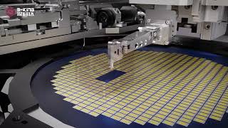
S-King Product: Flip Chip Die Bonder (High Precision Solution)
Просмотров 15 тыс.11 месяцев назад
Company: SHENZHEN SKING INTELLIGENT EQUIPMENT. CO., LTD (stock code: 688328) Sales Contact: ...

【半導體科普】台積電積極布局的 CoWoS 是什麼?AI 晶片大咖 NVIDIA、AMD 都瘋搶
Просмотров 203 тыс.9 месяцев назад
AIGC 與人工智慧等相關應用正在高速發展,因此設備端對於核心晶片的效能需求也越來越高;追求透過先進封裝技術提升晶片之電 ...

A Brief History of Semiconductor Packaging
Просмотров 181 тыс.Год назад
Links: - The Asianometry Newsletter: asianometry.com - Patreon: www.patreon.com/Asianometry - Twitter: ...
![[Eng Sub] TSMC SOIC](/img/1.gif)
[Eng Sub] TSMC SOIC
Просмотров 17 тыс.3 года назад
1. TSMC SoIC? 2. Process : Step 1. CMP (Chemical Mechanical Polishing) : Step 2. Surface Activation by plasma : Step 3. Chip to ...
어드밴스드패키징 CoWoS란 무엇인가? | 인포마켓 강용운 대표
Просмотров 48 тыс.Год назад
인포마켓은 종목에 대한 정보를 드리는 것으로 투자에 대한 책임을 지지 않음을 정중히 알려드립니다. #한미반도체 #TSMC #CoWoS ...
2.5D ICs or interposer technology
Просмотров 31 тыс.12 лет назад
What is an interposer technology and how does it work ?
[Eng Sub] TSV (Through Silicon Via) - HBM, Silicon Interposer, CMOS Image Sensor, MEMS
Просмотров 22 тыс.3 года назад
Semiconductor packaging technology for high performance application. It is usually used for high performance computing.
[Eng Sub] TSMC InFO Fan Out Wafer Level Package-Apple iPhone, Package on Package
Просмотров 21 тыс.3 года назад
This is simplified process flow. No. 1. Carrier preparation, No. 2. Seed layer deposition No. 3, Through InFO Via plating, No. 4.
【曲博Facetime EP59】台積電CoWos封裝技術與InFO差在那?SOI要怎麼做?
Просмотров 40 тыс.4 года назад
台積電的CoWos封裝技術與InFo封裝技術差別在哪? 曲博 Facetime 每個禮拜四晚上在這邊跟大家見面,聊聊最新的科技,掌握最新 ...
想進台積電先進封裝廠?推動摩爾定律「2.5D&3D封裝技術大揭秘」CoWoS InFO是什麼?WLCSP晶圓級封裝?AI晶片大廠輝達、超微愛不釋手系統級封裝?
Просмотров 43 тыс.4 месяца назад
今天的影片主要是想要跟大家分享半導體先進封裝製程✨2.5D&3D封裝的介紹✨ 二十分鐘弄懂半導體先進封裝(3D封裝),保證一定聽 ...
Dr. Lee's Math Series, Semiconductor (10) - Packaging technology, CoWoS
Просмотров 1046 месяцев назад
We explain the latest technology of C0S0W packaging.
Foveros Direct: Advanced Packaging Technology to Continue Moore’s Law | Intel Technology
Просмотров 34 тыс.2 года назад
Foveros Direct is Intel's next-gen advanced packaging that allows for more flexible and tighter integration between tiles. Instead of ...
17 반도체 패키징 TSMC 패키징 기술 CoWoS -인하대학교 주승환교수
Просмотров 2,7 тыс.Год назад
16 Chapter 에서 추가가 되었습니다. 전세계 최고의 기술력인TSMC 첨단 패키징을 알게되면 모든 패키징 기술을 다 알게 됩니다.
【半導體科普】4分鐘看懂2.5D、3D封裝,台積電最夯先進封裝技術CoWoS、InFO、SoIC一次搞懂
Просмотров 9 тыс.Месяц назад
2. 5D封裝、3D封裝?傻傻分不清楚?還有CoWoS、InFO、SoIC一堆新技術層出不窮,讓人眼花撩亂。 今天,科技新報將用4分鐘教 ...
揭秘CoWoS製程 Revealing the Secrets Behind CoWoS Production
Просмотров 14 тыс.5 месяцев назад
... and equipment suppliers and CoWoS processes are divided into segments. Let semiconductor expert Professor Lin Jiatong and ...
半導體2.5D晶圓級封裝製程 "COWOS" #台灣 #半導體 #先進製程 #台積電 #晶圓 #封裝測試#衛星#cowos
Просмотров 25 тыс.Год назад
半導體2.5D晶圓級封裝製程"COWOS" Chip-on-Wafer-on-Substrate. CoWoS是 晶片-晶圓-基板 的縮寫,是一種 2.5D晶片封裝 ...
2 Packaging Process Technology Things about Cu fills defects in BEOL, RDL and TSV
Просмотров 3,7 тыс.Год назад
2 Packaging Process Technology Things about Cu fills defects in BEOL, RDL and TSV.
Semiconductor production process explained
Просмотров 433 тыс.3 года назад
Humble sand. This is what the building blocks of the future are made of. But making them is a long process comprising a great ...
[Eng Sub] Fan Out Wafer Level Package: Apple iPhone, TSMC InFO, Qualcomm
Просмотров 13 тыс.3 года назад
Semiconductor packaging technology.
The Next Big Wave in Chip Design. TSMC's WoW Packaging
Просмотров 74 тыс.2 года назад
In this video I discuss 3D microchips which will keep Moore's law going #3Dmicrochips ➞ Support me on Patreon: ...
HC33-T2.1: Advanced Packaging, Part 1
Просмотров 27 тыс.2 года назад
Tutorial 2, Part 1, Hot Chips 33 (2021), Sunday, August 22, 2021. Organizer: Ralph Wittig, Xilinx This tutorial discusses advanced ...
Surpassing the Limits of Moore's Law through "Packaging"?The Mighty Packaging Alliance of TSMC!
Просмотров 398 тыс.Год назад
00:00 Apple WWDC Keynote, Vision Pro, and M2 Chip 00:58 Advertisement Segment 01:32 Has Moore's Law Reached Its Limit? 03:43 ...
[Eng Sub] Wafer Level Chip Scale Package (WLCSP)
Просмотров 28 тыс.3 года назад
1. WLCSP : Die, Repassivation, Bump : Repassivation(PI, PBO - HD MicroSystems) : Batch Process 2. Structure : Bump on Bond ...
TSMC 3Dblox™: Unleashing 3D IC Innovations for the Next Generation of AI, HPC, Mobile and IoT
Просмотров 8 тыс.Год назад
TSMC's Jim Chang took the stage at the 2023 TSMC Technology Symposium to talk about TSMC 3Dblox™, a standard to address ...
UCIe™ Packaging Technologies Webinar
Просмотров 4,3 тыс.Год назад
UCIe™ (Universal Chiplet Interconnect Express™) is an open specification that defines the interconnect between chiplets within a ...
TSMC Ramps Up CoWoS Advanced Packaging Production to Meet Soaring AI Chip Demand
Просмотров 13111 месяцев назад
Help channel - www.donationalerts.com/c/petademon.
Wafer Level Package(WLP)l 晶圓級封裝 l Wafer Level Package l 封裝技術 l 高密度封裝 l 3D封裝 l 無線通訊封裝 芯片封裝 l 微型封裝封
Просмотров 10 тыс.Год назад
晶圓級封裝(Wafer Level Package,WLP)是一種相對於傳統封裝技術而言相對較新的後製程技術。它通過在晶片表面建立封裝 ...
NVIDIA Blackwell GPUs Delayed: What Went Wrong?
Просмотров 275Месяц назад
NVIDIA's highly anticipated Blackwell GPUs are facing over three months of delay due to serious design flaws. The integration of ...
CoWoS完整解析!台積電的最強武器,輝達、蘋果都搶著要,CoWoS到底是什麼?|數位時代Tech Away
Просмотров 80 тыс.Месяц назад
本集重點✨ 】 台積電是大家的護國神山!其中最強武器,就是董事長魏哲家口中,產能非常吃緊的,先進封裝CoWos技術。 魏哲家 ...
How are BILLIONS of MICROCHIPS made from SAND? | How are SILICON WAFERS made?
Просмотров 578 тыс.10 месяцев назад
Watch How are BILLIONS of MICROCHIPS made from SAND? | How are SILICON WAFERS made? Microchips are the brains ...