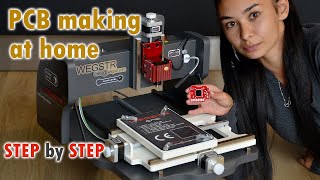
Making PCB with 3D printer and permanent marker

HTML-код
- Опубликовано: 9 фев 2025
- Using permanent marker, a 3D printer and etching to create a PCB.
I used FreePCB to create PCB layout and a gerber-file. I then used Flatcam to generate g-code for my K8200 3D-printer. A sharp metal rod is then removing the ink from the copper clad, and then it can be etched with ferric chloride. Tutorial: www.lamja.com/?...  Наука
Наука


![I.N "HALLUCINATION" | [Stray Kids : SKZ-PLAYER]](http://i.ytimg.com/vi/n5B5q1Hwt_U/mqdefault.jpg)

We didn't have 3D printers but back in the 80s we played around with permanent markers and used an HP plotter to draw the traces. It worked! Some markers worked better than others. We also printed thick film resistors and silver filled epoxy bridges right on the board with it.
I have an hp7475a plotter that I used for this exact purpose like 5 years ago.
God, people here seem to have no idea what is going on. It's a 3d printer with a pointed copper rod attached to the print head, it's not a CNC mill. He spread permanent marker across the copper clad board to act a chemical resist, preventing the etching solution from dissolving the copper. The rod on the printer is used to scrape off the marker in the areas he wants to be etched.
Amazing. A year ago i found your 20x servos code (really helpful), but never knew you also did this until just now.
I've been experimenting with making flexible PCBs outof aluminium foil & tape, etched with drain cleaner, but have been having trouble figuring out the best way to apply a resist. What you've done here is the closest i've seen anyone else get to my own project, and has given me some exciting ideas.
You just make the trace widths 50% (iirc) wider, then you have the same resistance values as a copper trace of equal layer thickness. Or even easier: keep your original PCB layout and just increase the aluminium layer height by 50%. It's not a problem. The problem is joining things (ie: components), as far as i can see soldering aluminium is a big pain in the arse.
Copper is a relatively scarce resource, i've become a bit worried about the possibility of the planet reaching peak-copper. IIRC there's only enough copper on the planet for every person to have a couple of kilograms each, it's going to be a problem, it will become especially noticable when we try to electrify the entire world's car fleet (which will happen / is happening already). Best to get ahead of that curve and avoid the problems. Aluminium electrical wire is already in heavy use for civil electrical distribution, because (even tho they use 50% more material than copper) it's more lighter weight than copper and is a lot cheaper.
Also i'd say that drain cleaner is a lot safer for the environment than ferric chloride, not to mention cheaper and easier to source. There's advantages and disadvantages, but in the long term we may not have a choice. So... best start getting some techniques hashed out now.
That is one of the best methods I've seen so far, besides the CNC method.
From all methods of making pcbs at home I tried this is the best if you have a 3d printer. End result is really good. Forget plotting with a marker, mounting milling capabilities on printers, toner transfer etc cause this one is easy and reliable. And as a bonus, the printer makes most of the parts you need itself. Tried it on an Ender 3 with great result from first run.
out there are many other methods of making a PCB, most of them more elegant and fast.
but this one sure as hell works with an excelent result.
scratching the surface with a metal rod ... talk about simplicity. nice job there.
Ah, It's a good time to be alive. This is so satisfying.
I love this.
Very well done.
A mini CNC mill is much easier to implement and it can also drill the through holes and cut the board outline.
And at about the same cost as a modified 3D printer.
Still, kudos to you for doing this, Lamja Electronics.
You are legend.
There's a lot of clever thinking that went into this. Thanks for posting.
I had this idea after seeing something similar done with a laser-cutter, but you actually put it into practice! Thanks for sharing!
Next, you should make a spin-coating machine to speed up the mask application step. You can get bottles of etchant-resistant inks. Try searching for "lumocolor" or "inkjet pcb".
I think you could use a good black spray paint or even a roller just to cover the board. Paint remover would be required at the end stage . I don't see why an expensive magic marker has to be used. Magic marker is probably cheaper for short runs though. The process itself is absolute;y brilliant and original, I am impressed by the creative genius of the process. This should save on the milling bits. Creativity like this is the soul of youtube.
This is probably obvious, but is it not feasible to just plot filament, possibly Petg, and then just wash away the uncovered copper?
interesting idea, i might have to try that.
far quicker..too, this isnt 3d printing its just computerized etching
I don't think it's possible, mainly because you need very high precision, 100% coverage of the area which is not etched, and the printed layer must be very thin. PCBs can be quite complicated, and I think it would need a lot of manual touch-up work afterwards. It would also be far more expensive... comparatively. As for the speed, well... that depends on your settings and controller.
What do you mean manual touch-ups? Does a 3d-printer extrude inconsistantly? Regarding thickness - how thin is the average 3d print head nozzle? It seems smaller than pcb traces.
Most are 0.4mm these days as standard, but I suspect also that such thin lines may struggle to stick to the copper surface properly, without some kind of adhesive, although large solid etched patches might stick okay due to the increased surface area. This is still a common issue on every 3d printer I know of, and you'll see on many forums that people go to great lengths looking for something to help their parts stick - for example, Frog tape, Pritt stick, PVA and water mixture in a spray bottle. Non-gloss ceramic works wonders due to its porous surface, such as the back of a bathroom tile. But yes it can be quite inconsistent such as going around sharp corners or just a single track peeling off where someone's fingerprint grease was left on a corner! Sufficient cleaning with isopropyl could prove me wrong, however, which I'd like very much.
A better solution may be to just clamp a finer marker pen to the CNC head and invert the print somehow.
Very nice idea :)
Now i just need a 3d Printer :)
Søren Reinke For smaller projects? www.dx.com/p/neje-fancy-dk-8-laser-box-laser-engraving-machine-laser-printer-for-diy-cellphone-case-384215#.VZKU4vlViko
Daniel Matthews That was my thinking too.
+Søren Reinke doesn't have to be just a 3d printer it can be a x,y, plotter as well
+Nicholas Finch in the mean time I have actually gotten a 3D printer 😊 but I'm planning on building an xy plotter just for fun.
What software did you use?
+Søren Reinke you can try this one
professormarlonnardi.blogspot.com.br/p/cnc-caseira.html
in brazilian portugues (sorry!)
It is a fantastic idea, I am testing it on a homemade machine, and it looks very good, as you said, an important point is the type of permanent marker used, thank you very much for sharing your work and design, greetings!
I did this on my Ender 3 pro and it works so well!!! No more laser printer nonsense ;)
Sorry, I just got a Ender 3 pro myself, and am hoping to use it for PCBs, why is it that this is better than a laser? I was under the impression that laser is the way to go?
@@contrabass8126 Laser is better, this is cheaper
@@contrabass8126 Laser is better. Higher DPI. 1200dots/inch gives you really god resolution and optically exposing will give you the best transfer.
It's cool. Also, I have a 4-axis CNC mill, so I could do the same, but PCB services, like OSH park are so dirt cheap and quick, and they do silk screen and solder mask, and they can do 4-layers, so it's just not worth spending the time to do my own PCBs.
Nice memories though. I made my first one when I was 10...
The result is too good for this method. I previously attempted the same with not much success. Good work. Slow yet good.
I have a T8 CNC machine and it is really messy and dusty milling a PCB. This method seems easy, tidy and quite practical. I might try this someday. Good job. Thanks for the idea.
Very clean result!
why not turning it to CNC?
This is Genius! I will implement this in my 3d printer, (Prusa i3) and try this at home !!!!
This would be perfect if there was some servo controlled arm with a sponge which could wipe the tip clean...
I think if you add the permanent marker to the CNC/printer, you could mark out the pathways and wash off all copper that isn't a pathway, like most standard PCB's do (for a good reason). Should also save you a lot of time, as you don't need to go back over a lot of lines again.
Agree - would much more sense
Also, not sure what the commands are in gcode, but I'd go looking for the Z axis instructions for the pen up/down. In HPGL is PU & PD - if you remove those from between the contour lines that are associated you'll be amazed how much run time it saves.
There's signage software out there which allows you to create a concentric router path which instead of being a series of concentric shapes is actually one continuous path along concentric shapes, I used to use software called Casmate Pro for doing logos for diamond drag engraving (which is effectively what you're doing) which produced much faster run times. ;-)
Автору огромное спасибо! Это то, что я искал! Если кто то знает лучший способ - пусть напишет! Автор видео показал лучший способ! Спасибо! Я мог бы и сам додуматься, но не додумался.
Really nice! Result looks good. I guess not to difficult to mount on K8400 instead of second extruder. Amazing.
theres a video and information on instructables..don't bother etching with ferric in a bath..just take a sponge and rubber gloves..apply straight onto the board and rub for 1 minute...use denatured alcohol to remove ink. I got a stepcraft cnc and will use that to drill out the holes AND plot the design. Your idea idea of a permanenet marker plotter pen is excellent..
Have you tried spray paint instead of a marker?
Jammit Timmaj No. But I tried glue stick and CA glue. They just scraped off in big flakes.
Jammit Timmaj Apply a static voltage. Dust it with toner. Apply the opposite charge on a very fine tip and pas it close to remove the toner were desired. This also allows you to use large bits to remove larger areas of toner.Then before touching it heat it with an infrared lamp secure the toner. chem wash and see what happens. I'd be interested to see.
+canadianman000 Why would you like to remove larger areas? From my point of view - the less removed, the less acid needed to remove it - the more PCBs you can make with 1 package.
+Robert Klauco
This is true, as much copper as possible should be left to conserve resources whether you are doing it yourself or having the boards mass produced. It's the responsible thing to do. All blank areas should be filled. Which also works out well for making fat power traces.
+canadianman000 in a similar vein, there is a craft product which is just coloured toner and a stamp-pad of clear ink. You use the ink to stamp invisible wet designs onto the paper, then sprinkle the toner on. The toner only sticks to the wet sections. You then heat the whole thing with a heat gun to melt the toner onto the paper.
Excellent!... I wish I had one of these machines in my times.
hi, it was very clever idea to print it opposite. i always thought of putting the marker on the print head, but using the rod actually is more effective, and gets rid of many problems ! brilliant ! :)
want to try this some day, after i master motor controlling with arduino.
+iceberg789 I thought the same !! using the fine tip to remove excess permanent ink is brilliant !
Outstanding idea and workaround. Thank you so much for sharing.
why am i just finding this in 2020?
Just found it in 2022, what have you made with your 3D Printer?
This is great! I might have to give this a try sometime!
Vinil cutter reused as a cnc for pcb, genius, thanks for sharing
тоже метод. Кто лазером краску сжигает, кто то фрезой со шпинделем (и травить не надо)....а кто печатает на принтере шаблон на плёнке, и с помощью фоторезиста создаёт себе печатные платы. Но некоторые в России уже обленились, и стали заказывать, отсылая по электронной почте только рисунок печатной платы.
I tried this method and it works pretty good. But why not replace the metal rod with a permanent fine liner and write all the PCB lines on the copper. You can do more passes to get a good line if necessary. Should be good enough for pcb's with not to thin lines. I will try it.
Looks like it worked great. How would I change my 3D software to do this?
i'd say this is more like a CNC machine than a 3d printer, cool idea though!
3d printer is a cnc machine
+rawux1228 that's right, but main difference is that 3D printer creates something by extruding/hardening something layer by layer, when CNC in general uses milling/cutting of solid material.
So, it would be better to say that this is general CNC, not a 3D printer.
No both are CNC machines. CNC= Computer Numerical Control. You can use CNC for any manufacturing process. The difference is one is a CNC Printer, the other is a CNC Mill.
You know what i mean't, So when you tell someone to go use the CNC machine, do they stop to ask which one, the printer or the mill? or do they go straight to the mill? Chances are they will go to the mill, probably every time!
Anyways, let me now revise myself to your semantics.
"This is more like a CNC Mill"
Since you're taking away material, not printing it.
Well, some shops have mills, routers, lathes, etchers, and yes 3D Printers. They are all CNC machines. When someone wants to use them you call them by what they are. Mills, routers, lathes, etchers, and 3d printers. When you're in those shops the CNC is implied.
This is very well done. Loved the video.
It looks good actually but your project does not require a high precision with thin pads and tracks like i.e. QFM packages.
The final precision will allways depend of the printer's precision.
A 2D laser with CNC engraver should be sufficient and may be cheaper for the same final result meanwhile this solution would work for those who allready own a 3D printer.
I havent thought of this, Ive been trying to cut with bits!. Thanks for posting
why not mount the pen in the printer and have it draw the tracks straight on to the clean copper? ...that's what I do, and I get very good results.
+Gabriel Rd smaller trace. I think the the tip of the pen is quite large for delicate trace of SMDs and QFP etc.
Lâm Đặng OK, thanks. I might try out your method to see how it goes.
how big is your pen point?
Awesome my good friend. very well done.
good method. I liked very much your idea. I'll try your method with my cnc. I will first tracks and after drilling with cnc.
Very good. THAT would also work very well with DyKem.
pretty cool, now i'm wondering if the same thing would work using a laser to burn off the ink?
you can use photosensitive PCB material and use a Laser on that one ;) but I am sure u've found videos on that topic until now :p
Nice idea, thanks for the inspiration ! never thought of it, thank you
This is the most amazing idea I've ever seen THANKS A LOT!!!!!!!!!!!!!!!!!!!!!!!!!!!!!!!!!!!!!!!
Interesting method! Did you tried to print with PLA directly on copper, then etching?
Is that a serious question?
@@alejandroperez5368 Yes, it is, I'm just curious to know if PLA will adhere on copper.
@@ricardobraganca2307 What if it adhered to copper? The resolution is very poor, even if you use a 0.2mm nozzle. Not to mention that PLA wouldn't last very long during the eching process.
@@alejandroperez5368 , I disagree. I think PLA should resist the etching similarly to toner transfers and markers, they are all plastic. Also a 0.4mm trace is very fine for a PCB, so resolution should not be a problem. The main concern is if PLA will adhere to copper or not.
@@ricardobraganca2307 0.4mm is not fine at all, it's quite coarse actually for PCBs. CNC isolating milling use V-bits with 0.1 and 0.2mm tips.
I'd probably go for a Dremel engraving bit coupled to a small 380 sized RC Car motor.
Worst case scenario is the bit just scratching away the marker *in one pass*.
Best case scenario is the bit also carving away the copper underneath.
Similar to what was shown one could adjust the desired result by a rubber or, preferably, a spring to give in.
How did you drill holes? And if I want to make a double -layer pcb, how to metalize holes?Thx~
Nice work ,could you describe how you did it, and what programs do you use?
radu - ionel rusu Hi. I used Flatcam to generate g-code. flatcam.org/
pilleyuppo23 i tried to load the file in pronterface, but it did not like it. what software did you use to send it to the machine? I have a ultimaker and i'm on ubuntu 14.04
Simon Claessen found it: bCNC. works as expected.
Simon Claessen Hmm after fixing my printer for a whole day, bCNC is not able to communicate with the printer. pronterface has no problems, but cannot send the file...
Have you tried to drill holes of the PCB with the 3D printer?
What about mounting a fine-tip sharpie to your print head and drawing out the traces?
brainfarth I tried that also. But this method is more accurate.
Could you please try making pads for package LQPF208 and post the result. I' d appreciate it as I am deciding to buy PCB milling machine or should I rather buy 3D printer and use your method.
+Žiga Lausegger I guess a proper PCB milling achine is better than this.
+Žiga Lausegger You're not going to get anything QFP reliably made using this method. Get a mill.
+Žiga Lausegger Arduino QFP puu.sh/n2s9Y/5737ceb865.jpg flash forge with sharpened rod and marker.
Thank you.
Have you tried with a laser graving machine to remove the ink? It could be more precise.
Good idea. This is the super brain from basic work.
Hello, this was so good to watch! I am quite new to it all and don't quite understand how the final product works. Say I put a +ve wire in that first hole above the first W, and a -ve wire under the last M, I can see that from the design the intention is that no current should flow. But as the PCB has depth, wouldn't current just flow through the inner material of the PCB anyway? Sort of like the ice cream in an ice cream snadwich, it runs all the way through the middle no matter what shape the biscuit either side of it takes up?
Now I'm hungry :)
+Mirandorl
The board is then submersed in ferric chloride so all of the bare copper is etched away. The ferric chloride can't penetrate the permanent marker and so that copper is left behind. Acetone can be used to wash away the black thus producing a pcb.
+Peter Lawrence true, but the result we see in the end of the video. If the chloride etches the copper away and afterwards we clean the marker away, we would have some wierd lines?
the cooper between the black lines should be keept right?
+Mirandorl The thing is, the thin layer of copper on top has been etched away. Think of it more like this, you have a plate covered in ketchup, plate being non-conductive, ketchup being conductive. The etching would be like you drawing a smiley face in the ketchup with your finger as to expose the plate. Since the plate isn't conductive, the "etched" parts don't allow current to pass, thus you have created a very messy PCB.
Nicely done! This can also be done using laser correct?
This is pretty cool!
But it is taking the least slow part of PCB creation (uv activatio and developing), which takes around 2 minutes, and making it unnecessary long.
Excellent Idea. Pity that I disposed my K8200 because it was so big for the small printing volume of 20x20x20 cm. The latest printer I have, is not much bigger, but can print 10x bigger (40x40x50 cm), has excellent printing quality, almost no noise, and cost me in 2020 half of what I paid for the K8200 in 2014. Still have the K8200 parts. dedicated compact PCB workstation would be maybe a good idea.
Does the marker need to be a certain type or have a certain chemical ingredient in it that you know of to be resistant to the etching? I'm just wondering how clean it would be if you had done an exact negative of what you made here... because obviously you have made an opposite of what would be a useful pcb right? Very nice though and just shows that with any machine that has x, y, z control, the possibilities are far beyond the recommended use. Good job.
+3D_ Tech this isn't a negative. You only need to remove a copper border around each trace, and that's what has been done here. There's no need to remove any more, it would only waste time and acid.
Another method of creating PCB......COOL!!!
But there will never replace the old school laser toner heat transfer etching process.
challenge accepted ;D (i switched to this: ruclips.net/video/HBIxvwZ_0og/видео.html , after watching search for my comment there 2 years ago)
" old school laser toner heat transfer" If that's "old school" you're making me feel ancient. I used to plot the layout on paper with an X-Y plotter at twice the size, photo reduce onto a transparency, fasten that to photo-sensitive copper clad board, expose to UV (?) light and then etch and wash.
hi! excelent work! did you change anything on the marlin config? or the software recognise it?
Carlos Guerrero Hi. I had to change the g-code generated by FlatCam a bit. I replaced all "Y" with " Y" to get a space between x an y coordinates. I did nothing to Marlin.
pilleyuppo23 What diagram did you use for it to print?
nice work,good idea,you need to do a tutorial because is great!
What did you used for corosion? I tried so much markers but with feric cloride it removes areas of the marker paint aswell
The problem is when you try to etching the pcb you need to wait without rubbing with a sponge if you want to make the etching process faster and you decide to rub with a sponge the permanent marker can't hold, I tested permanent markers many times and made on my PCB little holes because the permanent paint can't hold friction
just heat the acid bath, and use an air bubbler. You'll get a crisp etch in under 2 minutes.
Paul Frederick I use worm etching but i don't use air fish pump bubbler :D I like to process myself the pcb with some gloves and moving the PCB up, down, right, left and use sponge to rub the rusted areas making the process really fast, the last time i remember 2 min etching was on a 2x3cm pcb :D if you get a 10x10cm you will wait way more.
Domino60
yeah rocking sucks compared to bubbling. Entrancing air makes a huge difference. The pros spray. But spraying causes some problems. Having a pressurized system that can handle corrosives is problematic. Bubbling is almost as effective, and a lot simpler for the home gamer to do. As far as how hot to run goes, when you see fumes rising you're running hot enough. For Ferric Chloride that is about 110F
Paul Frederick I use worm water to prepeat my etching, put some gloves and work on that circuit till it's done, with a soft sponge slowly cleaning and shaking the circuit on the solution, it takes about 5~10~20min depends on how big is the circuit and one or double side. I use this and got no problems.
Domino60
get a 12V emergency car air compressor. You can usually pick one of those up second hand for next to nothing. Maybe a buck? Then just cut off the air chuck, or get a tire stem that you can put into the chuck. Some creative plumbing with plastic tubing (look inside spray cans for tubes) finishes your build. I use the cap off a spray can as my atomizer. Put that into your tank, and you're bubbling away! The 12V compressors are so lousy they put out pulsing air, which for bubbling is great. That unevenness really adds to the effectiveness of it all. I have a real shop air compressor with a regulator that I could use. But I prefer a 12V compressor for etch bubbling. Just for the pulsating choppy air it puts out. Do it. You won't be disappointed. You'll never have to rock, and sponge ever again. A lousy 12V air compressor can do all of that for you. The crappier it is, the better. Mine the crank broke in it, so I made a new one out of a nail. Which made it even crappier. Winning!
Why not use photoresist and add UF LED on the moving head?
+Artem Kuchin I mean UV LED :)
You need a Lamina tor
awesome idea!
This kind of crap is why I don't sleep at night.... Too much shit to make.
+Lord Pyrex seriously I always feel overwhelmed at the amount of things to make
Tell me about it
This tool will give you a chance to have long a sleeping nights :
check this out intmindsco.launchrock.com
Lord Pyrex
Exactly
use "sleeping lube pro" and relax
Spray paint or engineering blue may be faster to coat the board.
Very cool. I would think the 3D printer filament directly printed would also work.
Yes, I have been trying to find an answer to that question for quite some time now. I can not find any youtube videos, google searches or anything demonstrating ANYONE trying to print the etch release traces from 3d printer direct to copper. Do you know if that actually does work?
One method I used to make PCBs for many years was to use a transfer sheet. It acted like wax paper, 8.5 x 11 that you load into a laser printer (only) and print a reverse image to it. You then lay the sheet over the copper and iron it on from the back side. The reason it worked is because laser printers use something more like plastic or wax, not ink. That's why I assume filament will also work. You can get the transfer sheets here: www.allelectronics.com/item/tek-5/techniks-press-peel-pc-board-kit/1.html
Erich, not sure how that name got attached to my response about the transfer sheets.
Ron - you were receiving notifications that a reply was made, regarding using a printer filament direct. I was actually interested in knowing about that.
Vincent: Thank you for the information. I am not interested in toner transfer methods. Toner, by the way - is powdered plastic with a positive charge. By way of electrostatic, the toner will gravitate to the magnetic field onto the substrate (paper) then fused to that substrate by a Teflon coated hot fuser roll. Toner is very much like powder-paint.
Erich, I wrote those words. I was sharing that experience with you to explain why I believe filament will work as an etch resistant. For the same reason laser ink works. I was not suggesting you do anything other than 3D print a PCB.
I wonder if this technique can be used for double sided pcbs
+Charles McBoy It can. Just do one side at the time and make sure it is centered correctly.
Impressive, though I will most likely continue to use ink printing method but this does look well done. You also really don't need a 3D printer for this as a 2D machine more like a printer would work just as well. Might be even cheaper to build but would have the downside of not being reusable.
Nice work.
Hey, If I want to export Gerber from EAGLE which cam processor should I use?
Im sure you will be faster if u use a PCB with foto active skinn and then make a print with UV light. Tought u use it to remove all copper, what would make sense, about then is no chemical need.
this is good for single sided, but i'm taking this idea to the next level using the black marker and similar engraver, but 3D printing a bed of tubular supports and two of the supports have designed into them counter sunk 5.5mm socket head M3 screws used as alignment pins for double sided or multi-layer fast prototyping using multiple size PCB rivets and 0.6/1.0mm copper solid rivets made from solid wire. good enough for prototyping
Parabéns gostei muito do seu vídeo apesar de ser simples adorei, seu vídeo mostra uma outra maneira fácil de se utilizar uma CNC.
did you tried use wax instead of marker?
We used wax for etching (engraving) mineral glass. (with acid)
Thank you for posting this idea!
Can you purchase these printers from shops for personal use? I wish they were around $100.00 AUD or less. I want to get one for making my own PCB's . Do you think if i apply solder onto a circuit board, it will turn into a wire through the pcb
Raghav Sood Look for the 2 sided demo from Voltera. Their machine uses conductive ink and solder paste. I'm not sure if it's the paste or the ink but they fill in the vias to bridge the traces. Some real ingenuity going on with the desktop machines nowadays.
WOW !!!
Why did not I think of that?
Thanks!
:)
Great work but i'm wondering why did you use a marker and then etching ? Is milling made by the printer not enough ?
Abdullbasit AlHaita I did make a milling attachment for my pritner also. But it's a big mess. And noisy.
cool , i was going to just tape a sharpie to my head and put a few mm z offsetset and try that !
Saw someone suggest using paint and a brilliant idea formed. You can spray paint it and then scratch off the paint with the machine and etch it. After that you can scratch away the paint from the solder pad and have a beautiful solder mask left. Isn't it wonderful?
That's what Ben Heck did. Spray paint is definitely the way to go if you're dead set on wasting your time like this.
WOW....I have been looking to construct somthing similar, and there are a lot of ideas, but this one its realy simply and so good thing. Next week I am going to buy some material and make the same project. Thank you so much to share this wonderfull project. Best regards from Spain.
The metal rod, has a spring to avoid damaging the copper plate right? What 3d printing parts you use to adapt your rod on the K8200 3d-prineter head? (can you share it?)
What the material of your "sharp metal rod" steel? copper? the wast of ink dont
it takes lot of time (about more than 5x times if milling it, right?)
Does not the paint residue dirty the metal rod? You dont need to clean the rod from time to time to avoid accumulating the ink residue?
Was the printer cutting the copper? It looked like it was just scratching off the permanent marker.
Yes, pretty much. Any copper exposed would be etched away by the acid later.
It scratches the copper, but it's only incidental. The point is to cut through the etch resist.
Muito bom !!!! Parabens !!! E obrigado pela ideia !!!
Very nice. But how do you get the holes in the gcode file? I am using FreePCB as well, but don't see any holes in the pads in Flatcam. I have already updated my 3d printer, based on the info on your site, so i am able to start now...
aren't the holes is the drill-file?? Did you combine them?
You'll need to turn "pilotes holes" on in FreePCB.
Thanks! That did it! Now i can start tinkering...
couldnt you just scrape of the copper down to the pcbmaterial? no need for chemicals or anything? or does it peel off then?
+gamerpaddy that is hard to do, usually a spinning bit is required. and most of the time that just destroy the bit.
Can you try wax instead of permanent marker.
For small PCBs, its not worth the time to design and build a PCB, when I can wire it up and solder it in less than an hour.
Then again, I am practical and not into vanity and flashiness.
is this a working circuit board or just a proof of concept?
Aris Taukulis Both. The board is a servo controller. With an Arduino Pro Mini soldered on it.
Brilliant! You get a subscriber!
eres un genio, tenia una idea similar pero usando un laser para quemar la pintura, saludos
Sry if this is a dumb question but is there a layer of non-conductive material between 2 copper plates? When I watched I thought it was just engraving a solid copper plate and then that didnt make sense to me
Yes, I have a similar PCB and it's fiberglass that has been plated with a thin layer of copper on one or both sides depending on the board you buy. Obviously for simple circuits the single side board is cheaper.
There's only one copper plate on this pcb. The engraving is just scratching away the marker and then the chemical etches away the exposed copper. Problem is this sort of chemical is extremely hazardous, and it's easier to do this with a 2D printer anyway, so kind of a waste of time. If you want to use a 3D printer to make a PCB just have it remove the copper directly.
I'm kind of astounded at the comments here... Half of them are saying "why not use a marker" or "why not use a Dremel?" it's not the questions aren't valid, but they've been answered over and over in the comments. beyond that I would have assumed that the kind of people watching circuit board Production videos would understand how in precise something like a Sharpie can be. I also sort of thought that they would understand how flimsy most 3D printer frames are. really well done video dude. I don't have an actual printer only a 3D printer these days and this is brilliant. Definitely going to give it a try. :-) you don't happen to have STL files of the bracket you use to hold the Scribe do you?
Tutorial: www.lamja.com/?p=635 stl-file: www.lamja.com/blogfiles/3D_Printer_PCB_maker_steel_rod_holder_for_K8200_all.stl
Lamja Electronics oh! I didn't see the tutorial link.. thank you!
I'm astounded that people are impressed by this. Laserjet printer will give you same or better results for cheaper and 100x faster...
couldn't you swap the sharp bar with a dremel tool? and etch the board? I never done any PCBs . but it looks like you could.
a 3D printer's frame is not designed to handle the torque of a spindle. but maybe if you'd use a small one, it could work.
doubt it, there would be run out... enough to eliminate the viability of it in the first place.
Great idea!What is your pcb software?
I used FreePCB for this. But I have started using Kicad instead.
Where on earth am I supposed to get that thingy u start off with
Thats really nice work. I wish I'd thought of this before using a coupler to join a Minicraft pointy routing bit to a big DC motor and printing a mount for it. I've got a whole load of chemicals and a handmade developing box laying around doing nothing...
Thats not sarcasm by the way. There are some things you cant do a neatly with a mill, even if you do just shave the copper off with it.