When the professors haven’t been in the industry ever, and they wrote the text book they teach out of, that’s what you get 😅 Universities are so broken.
This is PCB design gold. Saving this to reference over and over again. Lots of great information and it's delivered in a way that is easier to understand than digging through all my books. Thanks for this!
On resonances in cavities and ground stitching vias. An analogy came to mind. It's like if you had a container with water. By swinging it back and forth with some frequency, you could easily achieve huge water oscillations. But. If you divided that container by partitions into many small containers, you wouldn't be able to achieve that huge water oscillations at that frequency. This is how ground stitching vias, by partitioning big cavities into smaller ones, prevent resonances in PCBs. Thank you, Robert, for your videos! They are extremely useful.
The most informative video on PCB design I have ever come across. You asked the right questions, and the guest was very experienced and prepared. This one should be included in the curriculum for any aspiring PCB Design Engineers. Thank you for the great work.
You have done so much for the PCB community. Thank you! And thank you, Rick! I do have a comment about routing high speed signals in the middle of the board (in order to get the power delivery near the surface). At speeds above 10gbit the via stubs will create significant problems (reflexions) which will require backdrill.
@@RobertFeranec the via stub length creates a reflection that can destructively interfere with the signal wave passing through it, basically the via stub looks like an open circuit and thus it reflects the signal back.
Awesome! This took me few hours to pause and fast backward just for jotting down the super important notes.😍@@RobertFeranec I indeed learned more than I imagined! Thank you so much !
@@RobertFeranec This video are too long For beginners or not tooo much interested to study deeply Can you please Write vedios Summary in discription So we can understand what is advantages and disadvantages of topic Like here Putting gnd
This is a very important job you're doing, Robert. It's great that there is now a good source for all the nitty-gritty details of designing a good PCB. Kudos!
Very very very very very and again very good! Thank you Robert and Rick, this video should be like a mantra for a PCB designer! And remember, the energy is... on the field!
I am so grateful that I found your channel! I'm a hobbyist with no formal education. I've learned so much from your videos. I've only ever designed 2 layer boards, but am about to start a project needing 4 or possibly 6 layers. I found you just in time! A lot of what you cover is over my head, but the principles are easy to understand and I'm better for it! Thank you!
You have done so much for the PCB design community and the people who are new to this that saying thank you would be an understatement now. Please keep doing the great work and teach people how to be a good electronics engineer. Love to Rick Hartley and you both ❤️.
Incredibly valuable knowledge shared in this video. This will change the way I tackle my board stack-ups in the future, although I can't imagine I'll ever need to worry about such high density concerns. Definitely this should give me more confidence when I press the "place order" button.
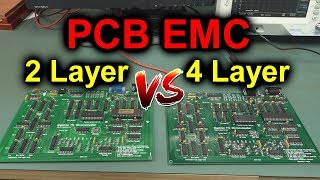
Thank you Robert, for sharing this video conference with Rick. Even though I am not into multi gigabit designs it made me more conscious of the effect of fast rise times. Most of the boards I design are 2 and 4 layers and looking at this video made me realize I have to be especially mindful of digital signals with fast rise times on these low layer count boards and minimize the EMI effect. Thank you for that.
I am the same, and this is why I always encourage people to still watch these kind of things. There is always something you can learn from it. I am also gonna change my work flow a little, first starting with rough layouting the board and second is to think about what stack-up I am gonna use and only after that continue with the rest of the layout.
I saw a similar presentation by Rick at PCB conference years ago. i was amazed then and still am now. Thanks for putting this up so i can re watch a million times =D
I’m a software engineer but always have been attracted to electronics. I have worked almost 4 years with low level embedded (bare metal) code for a payment related company. Loved reading datasheets and schematics. Passively learned tons from it (by asking myself what I was looking at and why it was done like this). I had to move to another field but still do a little arduino like stuff in my free time. Always wanted to give Kicad a try, especially since I got into the rabbit hole of custom mechanical split keyboards. Stumbled on Phil’s Lab videos. Next on Rick Hartley’s and now yours. Love Rick’s explanations and stories. He clearly is the rickiest Rick 🙂 Anyway I’ve learned a whole lot of exciting stuff thanks to you all. Kudos.
i took a pcb design class last semester at berkeley as an extension student. Easily one of the most valuable classes i’ve ever taken. They knew I wasn’t an engineering student, but welcomed me in anyways. They taught me how to use Kicad pretty fluently. The cool part is that we assembled all of our boards by hand after we designed them and ordered the materials; the class is jam-packed full of hands-on knowledge. I took the class at night after work, the course code is EE-198
@@soconnorivthank you very much for sharing this info! I’m French so I personally won’t be able to attend it but it will probably be useful to others, so thank you. It must’ve been great to assemble your own boards, thus making everything from the (properly) ground up (bad pun, I don’t wanna be grounded). I love the idea of designing a whole object from the pcb to the casing and programming the firmware. Everything can be done with open source software, even FPGAs (maybe old ones but still).
Thanks again for yet another great video! I just want to say that I really enjoy hearing about bad examples as well as how to properly do it. The section around 30:00 is great, we learn about a misconception ("we need to shield the signals!" vs "the signals need a return path"), why it was wrong and how to properly fix it.
... though I have a suspicion that "shielding the signals" (ie: preventing their electrical fields from escaping) is either the same thing as, or closely related to, "providing a return path" (for the AC current).
And that's why I like my 4 layer boards with ICs that have at least 5ns rise time. Anyway, thak you for very helpful video, I was always under the impresion that adding ground is pretty much always better, this makes much more sense.
It is great thing that you bring Rick Hartley to the channel, Robert. I really like the wondering video about PCB Layer with EMI issues. Thanks you both so much.
Now i Improved my all mistake while using (Ground AND Power) Plane onto 4 and 6 layer PCB... first i though it's don't matter or create EMI Problem if i select wrong Plane layer.. but i was wrong... i saw this video 3 times more for understand deeply.... Thanks you...you make my life...
This is a magnificent video, thank you Robert. Rick's explanation were so easy to digest. Great job, both of you. "Robert: how can you simulate this... Rick: Good luck!" This had me laughing hard.
Basically, pouring ground on signal plane can be a problem if you don't know what you're doing 🙃 For 4L board I put most SMD on L1 and r reserve L2 for GND (no signals at all) L1 for 90% of routing L3 primarily for power & secondary for GND reference of L4 (if possible) L4 primarly for GND and secondary for routing Final step: stapling all the gnd polygons with small vias 😅 So, basically, the 4L setup like (D) on slide 25, as shown 48:07 😁
Anecdote: one time I had to fix a layout mess of a embedded main board ~A4 sized with 400 components. The colleague was nearly "finished" (his words) and was taking parental Ieave. I strongly suggested to him beforehand use a 6L (and go to 8L if he has problems)...he chose a 4L, the GND/Power situation was horrible (signals every layer, split reference pours, ...) And I just had 3 weeks to fix that due to deadlines 🙃 Couldn't go to other stackup, as it was already reserved in the pipeline of production. As all components were on top I deleted all GND/PWR, and used strategy above. First taking care of important power and high speed signals. Due to the via power and gnd tacking it resultet in probably ~1600 drill holes (before it was more like 600 due to many the pcie connectors) That was an interesting summer😅
I was devastated when you jump 14 to 20 layer while i'm waiting hoping to see a design example for the 16-layer stackup structure towards the end of the video :D Luckily you exist and you are really teaching us a lot.
I have not done so high number of layers PCBs, but I would expect them to be similar to the last two stackups ... a lot of Signal/Ground/Signal/Ground .... ordering
What's the point? I can't afford anything above ~6 layers anyways for hobby, and the amount of time it would take to route 6++ layers would only leave this to companies and contracted professionals...
this explanasions were fantastic. I had lot of question about why the ground vias are required next to the some signal and all are answered. I appreciate your time for creating this video to share with others
I do appreciate the message that we should do simulation on high speed signal. unfortunately, it will be a long time till those simulation price come down enough for hobbyist to afford.
Hello, I've been designing two layers of protein since the program began. Thanks to your work and film, I won't be afraid to make the 4-6 layers I've been avoiding. Thanks to my movie buddy, he's as knowledgeable as you are. Greetings from Poland
Hi Robert, Excellent, thank you. Also, thank you to and Rick for sharing this information with us at no cost. Some have commented that the video is too long. I appreciate the discussion, even if it takes an hour or more, as the most important thing is to try and understand the concepts. Every board is different with different requirements and goals, and will require it's own set of compromises. Understanding the concept is the only way you can make those compromises intelligently.
Thanks so much, so much for sharing this precious knowledge!! It is not straightforward, considering the great amount of circumstances involved in PCB design.
Perfect timing! Actually, it was so great it kinda became totally intuitive now. At least for microcontroller level stuff. Gonna go revise my stackup... By the way, glad to see Fedevel logo on the presentation slides :)
The result of the discussion was that the tracks of the power and the ground should be close to each other to neutralize their field? So that their field does not affect other signals on the board? My English is weak and this is how I perceived it. thank u🙏🙏
Very informative and great video, thank you very much dear Robert and Rick ❤🌺 Please post more videos of engineers' work experiences and how to solve challenges.
Thanks alot Robert. You are providing such a valuable content. Listening to Rick and Eric always makes me learn something new about pcb design. Please try to comr with as much sessions as possible with Eric and Rick. Thanks alot for this valuabe information.
THANK YOU SO MUCH! This, though skyscrapers taller than my education so far allowed previously, "that said" all by itself brings me to a MUCH DEEPER understanding of the big picture here. ", having said that," is the 2020's replacement for "ummmm". ;-)
Thanks! This is a complete lesson on stack-up. Up to now I am not used to pour power on signal layers except near the input/output of voltage regulators or DC-DC converters
Cannot thank you how much I appreciated the video! I was watching all of your videos and they each add a slightly different perspective. I would actually really wanted to see some video where you design of a PCB with 4/6 layers with the in video suggested stackup, since it is a bit difficult to fully imagine how this should be routed: ----- Sig/PWR ----- -------- GND --------- ----- Sig/PWR ----- -------- GND ---------
I am a little concerned about power/ground pours on congested signal layers which is suggested on many of Rick's stackups. If the layers are very congested, there will be many small islands and strips of poured copper which will require vias so they aren't floating. It seems like those vias might take a lot of room and make it difficult to route the signals. Maybe you would need to use smaller vias to minimize this routing congestion. If you have a dedicated power plane, you can just drop the power vias pretty much anywhere, but in many of his suggested stackups the power is distributed on all the signal layers with no dedicated power plane. In those cases, you will have to line up those power pours on multiple layers to get the continuity you need. Seems like that might greatly increase the difficulty of routing the board. Your thoughts?
This is in my opinion your best video! It explains so many concerns about stackup which I had up to now and I would only hear some advises basing on "somewhere heard rules", which is very frustrating. Thank you!!
Valuable technical information Robert, the questions asked to Rick were really good. Rick hartley was just awesome. By the way, I use the same 10L stack up which you mentioned in the video.
@@RobertFeranec Also after watching this video, I am now very curious to watch your video on Flex PCB, I remember you have mentioned it sometime back that you are working on it. Hopefully we get to watch soon.
@@mdchethan Yeah ... I have not had time to work on the FLEX project ... I asked friend of mine to help me with it .. he is also busy. So, it is on my list, I am just not sure when exactly.
Robert, thanks for the sharing. Actually I got into problems on stack up design like how to arrange planes order and how to determine it exactly. I received heavy info form this video. Thanks again.
These are rules and guide (which i do practice them) but for practical case, there is a need to look at the boundary conditions on the signal traces, power and ground plane. There is always a trade off either you need to cut the number of power plane for signal or increase the number of plane (cost). But i prefer to have more ground plane than power plane.


They should teach this kind of stuff on the university. That's a thousand times more useful than most other things.
When the professors haven’t been in the industry ever, and they wrote the text book they teach out of, that’s what you get 😅 Universities are so broken.
I'm graduating in EE and I haven't had a single PCB layout class.
@@gustavrsh start making your own little projects!
@@p_mouse8676 Oh I did a lot of projects, but I never cared too much about EMC.
I designed, programmed and flew a model rocket flight computer.
"let's plug these equations for an hour... oh btw do your capstone and design a board now!" great joke education, great joke
This is PCB design gold. Saving this to reference over and over again. Lots of great information and it's delivered in a way that is easier to understand than digging through all my books. Thanks for this!
On resonances in cavities and ground stitching vias.
An analogy came to mind. It's like if you had a container with water. By swinging it back and forth with some frequency, you could easily achieve huge water oscillations.
But. If you divided that container by partitions into many small containers, you wouldn't be able to achieve that huge water oscillations at that frequency.
This is how ground stitching vias, by partitioning big cavities into smaller ones, prevent resonances in PCBs.
Thank you, Robert, for your videos! They are extremely useful.
The most informative video on PCB design I have ever come across. You asked the right questions, and the guest was very experienced and prepared.
This one should be included in the curriculum for any aspiring PCB Design Engineers.
Thank you for the great work.
You have done so much for the PCB community. Thank you! And thank you, Rick!
I do have a comment about routing high speed signals in the middle of the board (in order to get the power delivery near the surface). At speeds above 10gbit the via stubs will create significant problems (reflexions) which will require backdrill.
Thank you very much. PS: I am planning to make a video about via stubs and backdrilling
@@RobertFeranec the via stub length creates a reflection that can destructively interfere with the signal wave passing through it, basically the via stub looks like an open circuit and thus it reflects the signal back.
Awesome! This took me few hours to pause and fast backward just for jotting down the super important notes.😍@@RobertFeranec I indeed learned more than I imagined! Thank you so much !
My favorite guest, Rick Hartley!
:)
@@RobertFeranec
This video are too long
For beginners or not tooo much interested to study deeply
Can you please
Write vedios Summary in discription
So we can understand what is advantages and disadvantages of topic
Like here
Putting gnd
This is a very important job you're doing, Robert. It's great that there is now a good source for all the nitty-gritty details of designing a good PCB. Kudos!
it has been awhile, aside from your channel, I clap my hands at the end, which is unreachable on far too many other channels!
You Rock, Maestro!
Great video. Rick Hartley has really changed the way we think about EMI!
Thank you ats89117. I am very happy you liked the video.
Very very very very very and again very good! Thank you Robert and Rick, this video should be like a mantra for a PCB designer! And remember, the energy is... on the field!
Thank you Luca
I am so grateful that I found your channel! I'm a hobbyist with no formal education. I've learned so much from your videos. I've only ever designed 2 layer boards, but am about to start a project needing 4 or possibly 6 layers. I found you just in time! A lot of what you cover is over my head, but the principles are easy to understand and I'm better for it! Thank you!
Thank you very much Mark for nice words.
You have done so much for the PCB design community and the people who are new to this that saying thank you would be an understatement now. Please keep doing the great work and teach people how to be a good electronics engineer.
Love to Rick Hartley and you both ❤️.
Thank you very much Sameeran
Hi, Robert! Could you share with us the Rick's presentation on this topic? It seems to be extremely useful.
@@VeritasEtAequitas å
Thank you very much for your time and your video!! The title of my notes for this video: Print circuit board layer stack up (Gold dust)
:D Thank you Raul
Incredibly valuable knowledge shared in this video. This will change the way I tackle my board stack-ups in the future, although I can't imagine I'll ever need to worry about such high density concerns. Definitely this should give me more confidence when I press the "place order" button.
Thank you Robert, for sharing this video conference with Rick. Even though I am not into multi gigabit designs it made me more conscious of the effect of fast rise times. Most of the boards I design are 2 and 4 layers and looking at this video made me realize I have to be especially mindful of digital signals with fast rise times on these low layer count boards and minimize the EMI effect. Thank you for that.
I am the same, and this is why I always encourage people to still watch these kind of things.
There is always something you can learn from it.
I am also gonna change my work flow a little, first starting with rough layouting the board and second is to think about what stack-up I am gonna use and only after that continue with the rest of the layout.
Thank you Robert. Your talks with experts like Rick Hartley and Eric Bogatin are videos that I visit every few months. Very grateful...
I saw a similar presentation by Rick at PCB conference years ago. i was amazed then and still am now. Thanks for putting this up so i can re watch a million times =D
I’m a software engineer but always have been attracted to electronics. I have worked almost 4 years with low level embedded (bare metal) code for a payment related company. Loved reading datasheets and schematics. Passively learned tons from it (by asking myself what I was looking at and why it was done like this). I had to move to another field but still do a little arduino like stuff in my free time.
Always wanted to give Kicad a try, especially since I got into the rabbit hole of custom mechanical split keyboards. Stumbled on Phil’s Lab videos. Next on Rick Hartley’s and now yours. Love Rick’s explanations and stories. He clearly is the rickiest Rick 🙂
Anyway I’ve learned a whole lot of exciting stuff thanks to you all. Kudos.
i took a pcb design class last semester at berkeley as an extension student. Easily one of the most valuable classes i’ve ever taken. They knew I wasn’t an engineering student, but welcomed me in anyways. They taught me how to use Kicad pretty fluently. The cool part is that we assembled all of our boards by hand after we designed them and ordered the materials; the class is jam-packed full of hands-on knowledge. I took the class at night after work, the course code is EE-198
@@soconnorivthank you very much for sharing this info!
I’m French so I personally won’t be able to attend it but it will probably be useful to others, so thank you.
It must’ve been great to assemble your own boards, thus making everything from the (properly) ground up (bad pun, I don’t wanna be grounded).
I love the idea of designing a whole object from the pcb to the casing and programming the firmware. Everything can be done with open source software, even FPGAs (maybe old ones but still).
this Q&A style is very helpful, I only understood it the second time Rick has explained if after your questions
Perfect Video about Stackup! It solved my confusion about Stackup and SI issues inside. Thank you Robert! Thank you Rick!
I am a beginner in the PCB world and this video gives me LOT of knowledge about the LAYER STACK UP.
Thank You for this video.
Thanks again for yet another great video! I just want to say that I really enjoy hearing about bad examples as well as how to properly do it. The section around 30:00 is great, we learn about a misconception ("we need to shield the signals!" vs "the signals need a return path"), why it was wrong and how to properly fix it.
Thank you kbeckmann PS: Very good point with "we need to shield the signals!" vs "the signals need a return path"!
... though I have a suspicion that "shielding the signals" (ie: preventing their electrical fields from escaping) is either the same thing as, or closely related to, "providing a return path" (for the AC current).
Robert and EEVlog are my favorite EE RUclipsrs, but you two have very different styles...
And that's why I like my 4 layer boards with ICs that have at least 5ns rise time. Anyway, thak you for very helpful video, I was always under the impresion that adding ground is pretty much always better, this makes much more sense.
It is great thing that you bring Rick Hartley to the channel, Robert. I really like the wondering video about PCB Layer with EMI issues. Thanks you both so much.
Now i Improved my all mistake while using (Ground AND Power) Plane onto 4 and 6 layer PCB...
first i though it's don't matter or create EMI Problem if i select wrong Plane layer..
but i was wrong...
i saw this video 3 times more for understand deeply....
Thanks you...you make my life...
Great video! Your lessons and discussions are so valuable for me as someone just starting out with PCB design professionally.
I will thank Robert and Rick for there great content. A lot of people can use this information. Thank you!
Robert, you always makes videos few days later when I'm asking myself how to resolve a particular problem :D Thx!
I have similar thoughts ;)
I need to start recording sooner :)
This is a magnificent video, thank you Robert. Rick's explanation were so easy to digest. Great job, both of you. "Robert: how can you simulate this... Rick: Good luck!" This had me laughing hard.
Thank you very much for this video. Watched it without any pauses
Thank you very much Alex
I came back to this video to double check how to handle a 4 layer stack up, nice material, thanks !
Basically, pouring ground on signal plane can be a problem if you don't know what you're doing 🙃
For 4L board I put most SMD on L1 and r reserve
L2 for GND (no signals at all)
L1 for 90% of routing
L3 primarily for power & secondary for GND reference of L4 (if possible)
L4 primarly for GND and secondary for routing
Final step: stapling all the gnd polygons with small vias 😅
So, basically, the 4L setup like (D) on slide 25, as shown 48:07 😁
Exactly. PS: Also, sometimes pouring PWR instead may be the solution.
@@RobertFeranec Yes 😁
And I just got now at the position of the video which corresponds with my strategy: 48:07 (slide 25, stackup (D))
Anecdote: one time I had to fix a layout mess of a embedded main board ~A4 sized with 400 components. The colleague was nearly "finished" (his words) and was taking parental Ieave.
I strongly suggested to him beforehand use a 6L (and go to 8L if he has problems)...he chose a 4L, the GND/Power situation was horrible (signals every layer, split reference pours, ...)
And I just had 3 weeks to fix that due to deadlines 🙃
Couldn't go to other stackup, as it was already reserved in the pipeline of production.
As all components were on top I deleted all GND/PWR, and used strategy above.
First taking care of important power and high speed signals. Due to the via power and gnd tacking it resultet in probably ~1600 drill holes (before it was more like 600 due to many the pcie connectors)
That was an interesting summer😅
@@icestormfr Thank you for sharing.
@Robert Feranec it would be great if you could elaborate a little more on 4L PCBs. If you have google examples to share.
I was devastated when you jump 14 to 20 layer while i'm waiting hoping to see a design example for the 16-layer stackup structure towards the end of the video :D Luckily you exist and you are really teaching us a lot.
I have not done so high number of layers PCBs, but I would expect them to be similar to the last two stackups ... a lot of Signal/Ground/Signal/Ground .... ordering
What's the point? I can't afford anything above ~6 layers anyways for hobby, and the amount of time it would take to route 6++ layers would only leave this to companies and contracted professionals...
@@nameredacted1242Yes. That's exactly the point, lol
Wow, incredible presentation ... thanks Robert and special thanks to Rick for sharing his vast experience on the topic.
this explanasions were fantastic. I had lot of question about why the ground vias are required next to the some signal and all are answered. I appreciate your time for creating this video to share with others
I do appreciate the message that we should do simulation on high speed signal.
unfortunately, it will be a long time till those simulation price come down enough for hobbyist to afford.
I agree .. the software is not only expensive but also it is not easy to run and understand simulations.
Great video! TOO much information to process !
Thanks to Rick for sharing his knowledge!
Thank you Buk :)
Wow! Thank you Robert. This was a great amount of knowledge.
Thank you very much pgpiotrek
I'm learning enormous amounts here. Thanks!
Great lessons in how stackup affects board performance. Thanks
Hello, I've been designing two layers of protein since the program began. Thanks to your work and film, I won't be afraid to make the 4-6 layers I've been avoiding. Thanks to my movie buddy, he's as knowledgeable as you are. Greetings from Poland
thank you dseszef
Filling vias with peanut butter sounds tasty 🥜
19:40
I've heard Rick use that example so many times now, and it never fails to crack me up :D
:D
Hi Robert, Excellent, thank you. Also, thank you to and Rick for sharing this information with us at no cost. Some have commented that the video is too long. I appreciate the discussion, even if it takes an hour or more, as the most important thing is to try and understand the concepts. Every board is different with different requirements and goals, and will require it's own set of compromises. Understanding the concept is the only way you can make those compromises intelligently.
Really an expert! ... sorry I am from Denmark, but not employed in the mentioned company!
Wow, Robert and Rick, you guys blew my mind. I was hoping that I wouldn’t see one of my designs in Rick’s sin bin. Thanks again
thankyou for this great interview. This video is now the new reference for the future when we have to decide number and order of layers.
Thanks so much, so much for sharing this precious knowledge!! It is not straightforward, considering the great amount of circumstances involved in PCB design.
Thank you very much Emanuel
Federal. Such a great info packed interview w Rick. As usual. Took many notes. Please keep it up. I learn and relearn so much. Super fan, Todd.
Perfect timing! Actually, it was so great it kinda became totally intuitive now. At least for microcontroller level stuff. Gonna go revise my stackup...
By the way, glad to see Fedevel logo on the presentation slides :)
I am very happy you liked it Ilya. Thank you for watching. PS: yes, I noticed that too :)
The result of the discussion was that the tracks of the power and the ground should be close to each other to neutralize their field? So that their field does not affect other signals on the board? My English is weak and this is how I perceived it. thank u🙏🙏
Yes, I believe you understood the point, and if not, I’m in the same boat!
This is liquid gold. Thanks
This the video I've been waiting for! Thank you, Robert and Rick :D
Thank you very much Bradley for watching
All impedance is, is the size of the magnetic field compared to the size of the electric field. Thank you for saying it that way!
Yet another excellent video. This is one of the very few channels I enable notifications on, despite being subscribed to hundreds. :)
Thank you very much
Rick Hartley the man himself
Very informative and great video, thank you very much dear Robert and Rick ❤🌺
Please post more videos of engineers' work experiences and how to solve challenges.
Great lecture, thanks Robert!
Greeeaaaaat video!!! I love it!!! Thank you, Robert and Rick for sharing your experience!
Thank you Michael for nice words
Thank you Robert! Amazing interview with Rick Hartley
Thank you Krzysztof. I am very happy you liked it.
Thanks alot Robert. You are providing such a valuable content. Listening to Rick and Eric always makes me learn something new about pcb design. Please try to comr with as much sessions as possible with Eric and Rick. Thanks alot for this valuabe information.
Thank you Harish PS: I also learn every time I have a call with them
THANK YOU SO MUCH!
This, though skyscrapers taller than my education so far allowed previously, "that said" all by itself brings me to a MUCH DEEPER understanding of the big picture here.
", having said that," is the 2020's replacement for "ummmm". ;-)
48:23 for four layer PCB, I've got good information!! Thanks!
I am no where near this level of design but I feel like one day maybe I will remember this when I need to x'D
Absolutely amazing content on signal integrity mate.
GREAT video !! Thank you robert for making this happen and thank you mr.Rick for the information about layer stack-up and EMI problems!!
Thank you so much Robert and Rick for this great video.
Thank you so much Rick and Robert for this wonderful session 👌👌
The PCBWay add prior to the video was actually pretty rad!
This is gold.
very good video.thank you ferenac.
Hi robert and Rick, thanks for this video.
Hi Robert.
What a great video. This is something that we do not learn on university unfortunately.
Thank You
Layer number next the layer stack diagram will be really helpful. Excellent video.
Very good point. I was actually thinking about to add them in post production ...
Thanks! This is a complete lesson on stack-up. Up to now I am not used to pour power on signal layers except near the input/output of voltage regulators or DC-DC converters
excellent stuff, It starts me re-evaluating PCB design. Thanks, you guys are awesome.
This is very informative and simple to understand. Thank you so much.
Cannot thank you how much I appreciated the video! I was watching all of your videos and they each add a slightly different perspective. I would actually really wanted to see some video where you design of a PCB with 4/6 layers with the in video suggested stackup, since it is a bit difficult to fully imagine how this should be routed:
----- Sig/PWR -----
-------- GND ---------
----- Sig/PWR -----
-------- GND ---------
The video was awesome, Thank You and Rick so much ❤️
Thank you very much Alireza
Thank you a lot Robert and Rick
I am a little concerned about power/ground pours on congested signal layers which is suggested on many of Rick's stackups. If the layers are very congested, there will be many small islands and strips of poured copper which will require vias so they aren't floating. It seems like those vias might take a lot of room and make it difficult to route the signals. Maybe you would need to use smaller vias to minimize this routing congestion. If you have a dedicated power plane, you can just drop the power vias pretty much anywhere, but in many of his suggested stackups the power is distributed on all the signal layers with no dedicated power plane. In those cases, you will have to line up those power pours on multiple layers to get the continuity you need. Seems like that might greatly increase the difficulty of routing the board. Your thoughts?
This is in my opinion your best video! It explains so many concerns about stackup which I had up to now and I would only hear some advises basing on "somewhere heard rules", which is very frustrating. Thank you!!
Awesome
I liked this most and extremly useful.
Thanks to both .
Great video Robert and Rick! Thank you for the great insights!
Thank you Robert 🙏
such an amazing content !
Thank you Houssein
Excellent video. Very informative
Valuable technical information Robert, the questions asked to Rick were really good. Rick hartley was just awesome. By the way, I use the same 10L stack up which you mentioned in the video.
Thank you Chethan
@@RobertFeranec Also after watching this video, I am now very curious to watch your video on Flex PCB, I remember you have mentioned it sometime back that you are working on it. Hopefully we get to watch soon.
@@mdchethan Yeah ... I have not had time to work on the FLEX project ... I asked friend of mine to help me with it .. he is also busy. So, it is on my list, I am just not sure when exactly.
Robert, this was great. Thank you very much for sharing this great talk! best wishes!
very interesting talk by Rick!
Always excellent topics and videos, thanks for sharing such a great knowledge.
Awesome information. Congratulations.
Robert, thanks for the sharing. Actually I got into problems on stack up design like how to arrange planes order and how to determine it exactly. I received heavy info form this video. Thanks again.
Oh, that was so interesting! Thanks for sharing this with us!
These are rules and guide (which i do practice them) but for practical case, there is a need to look at the boundary conditions on the signal traces, power and ground plane. There is always a trade off either you need to cut the number of power plane for signal or increase the number of plane (cost). But i prefer to have more ground plane than power plane.
Very very nice video, thanks a lot for these very important informations Rick !
Extremely useful
Fascinating.
Very nice video..!! Thanks Robert and Rick..!!
Thanks a lot for the video! Very interesting.
Omg 48 layers! **wheezes**