EEVblog

HTML-код
- Опубликовано: 23 июл 2020
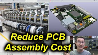
- Dave analyses a PCB layout from the EEVblog forum and covers all sorts of tips for SMD layout, component placement, routing, layer stackup, controlled impedance traces, supply planes and power bypassing.
Subscribe on Library: lbry.tv/@eevblog:7
Original forum thread: www.eevblog.com/forum/beginne...
Forum: www.eevblog.com/forum/blog/ee...
#PCB #Design #Tutorial
EEVblog Main Web Site: www.eevblog.com
The 2nd EEVblog Channel: / eevblog2
Support the EEVblog through Patreon!
/ eevblog
AliExpress Affiliate: s.click.aliexpress.com/e/c2LRpe8g
Buy anything through that link and Dave gets a commission at no cost to you.
Donate With Bitcoin & Other Crypto Currencies!
www.eevblog.com/crypto-currency/
T-Shirts: teespring.com/stores/eevblog  Наука
Наука


Young engineers will understand this and older ones might not but mentoring is so unbelievably important that I cannot stress it enough. This type of "Everyone grab a cup of coffee and head to the conference room in 5min" video is unbelievably helpful. Its literally like the boss told the group of junior engineers to head to the conference room to go over a random layout one of the new guys is doing to go over as a working example. This is crash course learning at its finest. Everything is boiled down to an essence.
Dave, you are doing a service. The floating talking head BTW is perfect. Anything else for a video like this just wouldn't have worked. Everything on this video was 100.
Thank you!
Yeah, can only agree and upvote.
I'm a logistic-programmer, the learning for my job where mostly some word/powerpoint-documents i found in the company-network and a few small courses. And i came right when they changed the software and team-assignments, so when i had a problem nobody even knew who i could ask for help. When the next 2 guys came into our team i had saved those documents that took me a long time finding (and that since have been deleted !!! even) and made sure to be there when ever they had any problems, constantly looked over what had produced and also gave them tips of helpful things (for example we have some small helper-libraries for stuff you need to do over and over again - but there exists no documentation for that).
Reviews and mentoring is worth its time in pure gold, if it could be monetized. More eyes,different skill sets and (prior) experience is the best way to debug 'whoooopsies'
I have a question though, why wouldn't older engineers understand the need for mentoring?
- They for one should know how inexperienced new designers are, but I guess some people will give off the impression that they know and can do it all - and hence don't need mentoring and reviewing. Anyways, those conference room meetings which lasts only a few hours imho usually saves days and countless hours of fustrating work down the line.
@@EgonSorensen *"
I have a question though, why wouldn't older engineers understand the need for mentoring?"*
Cause to them (or you) it might be "obvious".
had this a couple of times happen to me already despite already being very careful to clarify what i mean. One example is the terminology used in warehouses to describe the packages/cartons/whatever used to transport goods around the warehouse or out of it - there are several different abbreviations for that, some that are discouraged, some that have been used 15 years ago but supposedly no longer used and so on. I have worked with them, i know them, i don't think about them being anything worth mentioning.
But then it happens that for a new person you give them something like "this has been done for XYZ already - you can look it up there and try to replicate it here" and then they wonder what the hell those 3-letter-thingies are.
There is a reason why becoming a teacher takes quite some time. Once you have learned something you know how to do it - but that also means you are no longer in the position of not knowing even what to ask. Being a good mentor is not easy (and i certainly would not be a good one - i can only try to help for the few things i know they will struggle, but not nearly enough to get them started on my own)
@@ABaumstumpf "I guess some people will give off the impression that they know and can do it all - and hence don't need mentoring and reviewing."
- this goes especially for both new and experienced people
New engineers have their heads full of stuff they don't yet understand, making it hard to cram more stuff in there - so mistakes are (likely) made. It takes time to settle in.
Old engineers have had their seats for long, starting to take things for granted and what they have learned has become 'practically understood' - and they might have forgot how it is to be new at a task, so they take things for given - I agree.
I also have had the 3-letter word experiences, and it must have been a pain for some to explain what I asked about. It is a 'giving game' to walk the line, it's far from easy and not always fun and games - but then, that's engineering in a nut shell to me.
Older engineers will understand the value of this video. (Well, I do,.) It may actually be used in the conference room in some places. It should definitely be required viewing for any new engineers.
I have to say Dave, the green-screen was worth every penny in this vid, excellent placement!
I thought so! I'm enjoying the green screen, I think it works pretty well.
The placement just made sense here as there were no tracks in that spot.
@@EEVblog You should have flipped only horizontally, to mach your movements ;)
@Aidan Macgregor ROFL this is to prepare us to the red dot when Dave will be a transhuman.
@@b_force4079 Yep, agreed.
Dave should mirror the greenscreen Video from his head. This would allow him to look to the right side of his screen, wich would than match the PCBs right side.
Now it’s „wrong“ he looks to the right but explains something on the left.
I feel like analyzing designs & workflows is a really underrated kind of learning. Great video & thank you for sharing
Yes, almost nothing more valuable than competent peer review and critique!
Absolutely agree. This is literally the boiled down essence. Its the boss grabbing all the new engineers to the conference room to go over a design. Its great.
Especially workflows...
So true, would have killed for a class dedicated to this stuff in undergrad.
Seriously, the way you look down to the PCB from this little floating head is so hilarious! I think it's great :D
And cool content, thanks for that! I guess I kind of knew most of what you said in this video already, but it's still a very neat overview with a lot of reminders to the little details. Will probably help me with my next designs ;)
I like it too!
Some have said they find it weird and don't like it.
@@EEVblog
I love it, don't listen to everybody else!
@@EEVblog We can ignore those people, they are wrong.
@@EEVblog dave you gotta make the floating head into its own series, hilarious and educational
@EEVblog Hi Dave, would you tell us your capture software/camera setup specifically for this type of video? It’s quite an interesting format
Those decoupling caps around the image sensor looks like they are playing musical chairs.
Last one down gets the inductance!
@@EEVblog I think all of them got the inductance in this case!
@@EEVblog Is inductance contagious? In the new normal, it needs to be asked.
I was reminded of a May-pole dance. But where are the zeroes?
The designer probably had them right the first time but then decided to turn the chip 90° for signal routing "optimisation"?, but did not move the caps with it. Just guessing ofcourse...
Damn I wish I had seen this video 2 hours ago. I just submitted a project to JLCPCB and after watching this i see a few flaws in my design
same here lol
It's probably not too late to ask them to hold it until you send them a revised design, ask them :)
To be honest: Even if you are an experienced PCB designer, two hours after submitting the design, you always find flaws, artifacts etc.
You submitted - that is fine. Improve on the next revision. Revising a board usually improves the board "anyway".
Note that this is not only in PCB design: book authors review their work over and over again - that is most of their work - but when they receive their first production print, they will immediately find a typo.
@@equitimer that is kind of rude, as the design likely is already passed CAM and already scheduled in the panel. Either your design is ready for production or it is not.
If you have half-ready designs, ask for a design rule check and quotation.
As a professional PCB designer, I always want to finish the board design on friday, so that we can order it on monday. That might sound like waisting a work day - but in reality: Looking at a design with a fresh mind either gives you the good feel of "yeah - this is it" or the "crap - I need one more day to fix this mess". In case of "I need to this mess" loosing a day or two is still better then wasting a PCB production, assembly and board botching and board bring up time.
@@sarowie In principle I agree, but realistically - unless this was an express job it is highly unlikely that the boar was already inserted and committed into a panel just a couple of hours after being sent. Shit happens. So to make some changes to the layout shouldn't present an issue, especially if the board size and stackup were identical. At any rate I suggested he could ask....not demand.
it's 4 am at my local timezone and this video drops. nothing better to watch at the moment. i have no life.
Nerd.
I've just watched it at 3am haha
Same. Its 3:32am UK time when typing this comment
Great video! 10 most important PCB design rules by showing how not to do it. And after you explain it it's all so obvious. Thanks Dave!
Dave Jones is a great teacher and mentor. Very well spoken.
Green-screen looks great. 👍🏽 Can it be mirrored so your head moves with the point-of-interest? 9:35 you noticed it, my learning style really appreciates you using this.
Good point. Yes it can be mirrored easily.
Needs a green shirt for best floating head effect. :D
Turtleneck please
This series could happen more often, this is great learning from Dave.
Thanks, Dave! I'm just in the curious stage with wanting to start designing a PCB sometime in the future, and stuff like this is really fascinating.
I have plenty of other PCB layout tutorials as well.
@@EEVblog Thanks! I'll check them out.
I'll often connect bypass caps to an ICs power pins but not connect the pins to power until after an initial
placement of components on the pcb, that way the rast nets clearly show what pin an cap belongs together
thank you for the video, we really need more video like that. maybe some schematic review.
I did a schematic recently, but it was more BOM related.
Yes, I agree. A schematic design video would be great with some "best practices" for larger multi-page organization.
Thank you for this video, as an engineer i will highly appreciate more design videos and design's review as it gives more information to all of us.
I will also highly appreciate more advanced and complicated things for (non beginner people). Thanks for all the information you gave us all these years.
My boss is giving me my first PCB design project starting next week, this is perfectly timed!
How did it go?
All good advice Dave. The power wandering around on a 4 layer board instantly threw me for a loop (pun intended). 🙂
It looked like he tried to do the layout for a 2 layer PCB, then had to later change the design. Those 2-layer power traces definitely need to go in favor of vias to the power planes.
Your PCB layout videos gave me the confidence to design and build a PCB for a small project a few months ago, so thank you for the excellent content!
Now that I've been through that and have a grasp on more of the basics, I'm finding that I understand and even predict more of your advice. I'm looking forward to trying my hand at more complex boards in the future!
Always look forward to these Dave as you do point out the real nuts and bolts of good PCB layout Thanks
This is the kind of video that keeps me coming back. Awesome Dave!
The USB-to-Serial chip is CH340, and its CH340C version is exactly the same SO-16 as others, but doesn't need an external crystal, it has an internal one, the XTAL pins just stay NC! The chip is available on LCSC
Hmm I heard people say it's very unstable though, don't know why. That's why I just used the G version in a board a while ago
Internal oscillators have fairly wide frequency swings over temperature. I'd prefer to use the crystal for the much tighter frequency tolerance. USB doesn't like varying signal rates.
I've done several hundred boards with the 340C and generally it's been good for me. However I did have this one customer who absolutely could not get the products to operate on one of his PC. It could have been many reasons - including this.
@@Dave5281968 Wouldn't you rather use the host's time base in the device? Guaranteed to be ±0 variance from the host's time base, once the x48000 PLL locks.
@@AirzonesBlasters Yikes
These are definitely my favourite EEV videos. Great for two reasons; reinforces the things I do know, and it's rare I'll watch one and not pick up 2 or 3 new things. Love it. Keep up the great work.
This video is perfect! I always find myself learning the most by looking at existing electronics and studying how the traces are connected. Love the content, hope to see more!
This is an excellent piratical tutorial. I learned a lot in something I haven't had to think of in decades.
This was great, I'm working on a design now and you gave me heaps of tips I may not have thought of. Informative videos that help people with their own work are my favourite kind.
this is the sort of stuff that made me watch Dave all these years
This is absolute gold. Fantastic content.
I'm a newbie at doing anything with this stuff, and all these points that Dave makes provide a direction for how I can get better.
This kind of video was about 50% of the reason I subscribed. Thanks, it's been a while.
I especially like your ideology for routing traces. I will soon be laying out the first 4 layer PCB I've done in years and this type of video helps with remembering how to make the decisions with prioritization and overall layout.
Great, engaging content! Like the layout analysis and how it can be improved. Thank you for sharing!
Floating head looks awesome! :D Thanks for fantastic video! Lots of knowledge for newbies. Waiting for more such content.
Please do more of this....very interesting.
These types of videos I really enjoy - It's almost like having Dave as a mentor explaining what to do. Regarding the decoupling caps, I always like to think of it as knocking out any inductance that's introduced from the long trace from the power supply to the chip, placing the cap as close to the IC as possible means the trace post cap is super short (and therefore very low inductance!). But, the discussion on things like layer stack up and WHY you should have it that way is priceless, I'll definitely be watching this video again when I need to lay out another board!
Floating Dave ist ABSOLUTELY GREAT!!! Makes a very clean image and much room for the content.
I like the Floating Head overlay on the PCB graphics...Great PCB basics tutorial.
As someone who is only getting started, this is absolutely priceless. Thank you so much for making these.
As many other comments have said - great video! Love the content, very educational and informative. Also love the green screen!
Dave has finally assimilated himself into a PCB!
I love the green screen and floating Dave! always learn a lot from these, thanks!
I'm working on my first real complex PCB and this video will probably keep giving me good info along the way, as well as a good chuckle - floating Dave is great!
I have graduated a few months ago, but I've known you for years now. you are my role model Dave, please keep doing these. I have learned stuff that would've taken years of mistakes from these videos. thank you.
This is great Dave. I just finished a 4 layer board and I’ve picked up some good tips here for my next revision.
Green screen talking head rocks! Noticed it earlier in the video. Another great down under video! Thanks!
As a maker I am just about to plan my first PCB. Some days ago i did not have a clue how do that. So watched ca. 30 videos here on youtube... They all turned out to be just reportages. By that i mean they did not succeed to teach anything useful, i literally just could watch other people using some SW to draw a board, but none of them explained why and how they make design decisions, rendering all that stuff useless for educational purposes. Then i stumbled upon your videos about capacitors and then this one. I just can say thank you for these! Watching just some of your content made me understand the very basics of PCB design in a way that i think i have good starting point for now.
Loved it!
And the casual ".. and Bob's your uncle." LOL 🤣
I'd really like to see more of this.
Cheers!
Thanks - this was fun! I agree with many of your ideas on pcb design. This is where so many designs go bad.
This was incredibly helpful and insightful. Thanks so much for the great advice!!
I like how you’re talking a lot about having a best practice mindset. If you consistently do something even when it’s not required it becomes a habit.
I’m still new in designing my own boards so this helps a lot. It’s often the simple things that get you until someone points it out.
Oh and the green screen is a definite winner! I feel it all looked better to follow along this way.
Winner winner, chicken dinner 😜
I find these types of videos to be incredibly helpful and informative. I studied EE over 20 years ago and eventually ended up being a programmer for the last 2 decades, but I've always been a hobbyist in electronics. It's easy to build all kinds of circuits today with resources like Adafruit and Sparkfun modules. Just stitch them together and add a bit of code, but sometimes you have something that you'd really like to turn into your own board and this practical examination of a real world project is awesome.
I'd like to see a whole series of videos aimed at the amateur that covered duplicating the functionality of these modules into a custom board (within copyright and design practices).
Same here but 30 years ago.
Enjoyed the review... Thumbs up Dave :)
Excellent review. Learned so much! Thanks.👍
I really liked this one, and as others have said, covers off some basics that are common mistakes, even by people that have been producing boards for years now!
dave thank you so much. you are so good person for productivity.
Thanks Dave. I've learned so much from you!
This was so insightful! Thank you so much for your videos sir.
i really appreciate this content as a layout engineer.
Great video! Right to the point. Signal, GND, PWR, Bottom. Yep. And think of SMD as single layer. Right to the point!
Thank you very much sharing this. Just great
I would replace the micro, FPGA, and a USB uart with an STM32F4 or F7. As long as that image sensor spits out parallel data. If it has MIPI output, then you will need some sort of MIPI converter.
i just love your videos, you have such a nice way to explain things even complicated topics
Green Screen Excellent , Video Content Excellent. More of these Please
Great video. I've noted so many crucial points that you have highlighted. Definitely learnt something from this video. Many thanks :)
Great video. I would love to see the final revision of the board after your advise.
I never run tracks between pins, like on that lower left, unless absolutely necessary. It's easy to end up with whiskers to be left when etching the board. It's also not ideal to be soldering either side of the through trace because you can get a solder bridge if the solder mask isn't perfect. There's no need to have done that since you can route the power to avoid it.
This board uses very few hole sizes which is good. However, make the vias as big as you can, because small drills, say 0.4mm or less, have much shorter flute lengths than bigger ones. PCB manufacturers typically want to drill through 3 x 1.6mm boards in a stack because drilling takes a lot of time. As soon as you drop below 0.4mm, you're pretty much forcing them to drill them 2 or even one high. Ask your PCB manufacturer about this sort of thing, you can save a lot of money. Decades ago, all PCBs were drilled and routed 4 PCBs high, and via holes were 0.7mm diameter to allow that.
If you have lots of through holes, try to rationalise them to use the same sizes wherever possible. Again, PCB drilling machines have to stop the spindle, swap tools and then restart which all takes time. It's also another possible source of error, because drills can look the same size.
Another thing we used to do was to drill the first and last hole of every size in the scrap outside of the circuit frame. That way a quick visual check can spot if a drill broke. If there are thousands of holes, you won't spot this until much later in the process.
Again, ask your PCB manufacturer for their best design practices, and better still, go and visit them and sit down with the people who are the victims of your poor design decisions.
Use wide tracks rather than unnecessarily narrow ones, and don't route them up tight against things when they don't need to be.
Run a gap check, and increase the clearances it flags up. Increase the allowable gap clearance and do it again. That way you can make the board easier to make and have less chance of shorts or interference.
Thank you so much I'm a young electronical engineer and this will be sooo helpfull. PCB design is not well teached in school I think, all thesee littles tricks are new for me. Thank you Dave
WOW! \Some proper electronics on EEVB - been a while ;-)
love this kind of content, thanks!
Woow, great tutorial, thanks!
Dave, the green screen is a great upgrade...much more flexibility and makes room for activities.
I'm a shade-tree electronics hobbyist and I'm starting do build my first board in Kicad. It doesn't require any signaling, but I will definitely use your suggestions if I ever get to that point. Thanks.
Thanks Dave! Just like the old days.
Very interesting, more of this please! :)
Dave ótimo vídeo sobre layout . Sou apaixonado por criar layout e projetos para área de tecnologia. Ótimo layout. Abraço
Really great content. Thanks
Great video as always. Its a good idea to consider how your going to distribute the power during placement but I always route most to least critical IO then I circle back to the pdn.
I would really love to see you layout this circuit. Not that you need a complete stranger assigning you work but a before-and-after on this thing would be really informative. Thanks for the explanation.
Thanks for the video Dave. I learned many things today. I'd like to see more videos like this. I like the green screen too.
I loved this video, and the green screen. I especially love those Lattice FPGAs.
Haven't been at the channel for months. This video on its own is a quintessential distilled practical knowledge of PCB design.
Learned a lot.
Anyway, may I ask someone to suggest a good, up-to-date book (or course) for PCB design, please?
Helpful video. I liked it
thanks for the tips :-). more such videos please :-)
Great video, I learned a lot about multi layer boards. Floating Dave is awesome, but don't forget to mirror the cam image to match the screen content :)
I think the talking head is great Dave, Worked well. Nice video which is now making me revisit some of the stack-up in a 4 layer PCB I am currently working on so thanks.
Thank you, more videos like that please
Very interesting video!
very interesting and informative, thanks
Love the floating Dave thing !
I like this stuff. Do more such videos please.
I love this as a video segment :D It's a great teaching aid, plus people can submit their own designs! I know I got some PCB's I'd love you to have a look at :)
Also there's more immediacy to it, unlike a mailbag where stuff can get backlogged for months cause of delivery times and so on
Dave. Great video, particularly when taken with other ones that you've made on PCB layouts. I too like the floating head.
It would be educational to see your routing solution, even if incomplete, for this project. Of course I realise that this would be counterproductive for soFPG and for your time. Perhaps soFPG will put a revised layout up for further review because a followup would definitely be of interest
Beautiful example of why FPGA bypass caps are often placed on the bottom layer. Signal lines first, then drop vias to the bypass caps, and Bob's your auntie.
The DC/DC could also be improved. The input caps are far away, they should be priority one. Place them as close as possible to the IC and even connect their GND-pad directly to the IC without any vias. Also do not connect the feedback line to the inductor, connect it to the output cap instead. Additionally, I would rotate the chip to make the switching node as short as possible (prio 2 directly after the input cap).
I have a renewed respect for computer motherboards now. Routing traces seems to be quite complicated, with a lot to consider. I learnt a lot from this video - thank you!
I can't even fathom the amount of work in routing multiple BGA devices with hundreds to thousands of connections on each. I'm sure it takes large teams to design PC motherboards. I know I will never even attempt it or anything even close to it. Too confusing. Too many wires to route.
I'm liking the decoupled-head Dave
This was a great video, I learned a lot
Great Video!
Great video as always! One thing that struck me though that I was kind of expecting to be mentioned is the placement of the FPGA and converter each placed on opposite side of the image sensor
Just switching place between the uC and FPGA would help shift the ground-plane return currents (assuming there is a solid ground plane ofc) of the FPGA from passing directly under the image sensor
But thats just my own humble opinion :)
Keep up the great work!
Love this video
thank you for this video!
Interesting! - Been liking your green screen videos for when your commenting on PC content.
I used I2C IO extender for arduino project, it was around 1,5m away, coupled with standart cable, going power for it in same cable. Just needed to to drive data lanes bit harder (lower termination resistor values), working just fine, no need to worry about I2C lines on the PCB, they will never be so long. Just imagine how big a PCB must be for lines to be over 1,5m xD
Problems with I2C will usually show up quickly if you go do your proper EMC testing. It's easy to get your communication completely messed up when you apply some RF fields to your designs. Sure, it might work in your lab and on a bench, but if you have some radio emitters (like cell phones) nearby, your device might suddenly act all crazy... Seen that happen quite a lot on I2C, even on relatively small 4 layer PCBs with proper circuit and layout designs and ground planes.