Animation | How a P N junction semiconductor works | forward reverse bias | diffusion drift current

HTML-код
- Опубликовано: 18 май 2014
- Our Web site: www.techtrixinfo.com/
Plz follow us on Facebook: / techtrixinfo
Plz support our RUclips drawing channel: / ethanshowtodraw
This simple animation video clearly explains the topics P-N junction semi conductor or diode, what is forward bias and reverse bias, what is diffusion current and drift current, what is avalanche breakdown etc
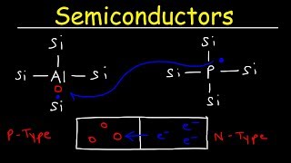
What is a P -- N junction semiconductor and how is it formed?
The PN junction semi conductor is a combination of P type semiconductor with N type semiconductor to achieve the practical utility of both. It's formed, when a P type semi conductor is joined to an N type semiconductor.
The P type semiconductor has free holes with positive charged and the N type semiconductor has free electrons with negatively charge.
What happens when a PN junction is made?
When P and N semiconductors are joined to make the PN junction semiconductor diode, the electrons near the PN junction jump from N to P and holes near the junction jump from P to N. This phenomenon creates a space charge region or a depletion layer as shown in the video. At this space charge region due to the movement we have electrons in P region and holes in N region. For some time the electrons move back from P to N in the space region or depletion layer and some holes move back from N to P in the space region. This continues to happen till equilibrium is reached. This movement of electrons and holes in the space region or diffusion layer gives rise to Diffusion current.
What is Forward bias and how does it occur?
Forward bias occurs when the positive terminal of battery is connected to the P region and the negative terminal of battery is connected to the N region. In this condition what happens is the positive terminal repels the holes towards the junction and the negative terminal repels the electrons towards the junction. Due to this repulsion, the depletion region or space region narrows down as shown in the video.
But at a particular condition, If the voltage in the forward bias is above a specified range, the electrons in the N region drifts through the junction and migrates to the P region and the holes in the P region drifts through the junction and migrates to the N region.
Now the current flows across the circuit and this current are called the Drift current.
What is Reverse bias and how does it occur?
Reverse bias occurs when the negative terminal of the battery is connected with the N region and positive terminal with the P region. In this condition holes (positively charged) from the P region get attracted to the negative terminal of the battery and electrons (negatively charged) get attracted to the positive terminal of the battery. This results in the depletion layer to widen up.
Now the PN junction acts as an insulator and will not allow any current to flow in the circuit. But at a condition, if the battery voltage is above a particular limit, which is called as the reverse bias breakdown voltage level. Electrons and the holes breakdown through the PN junction and cross over resulting in the current to flow through the circuit. This break down is called avalanche breakdown
In this process the current flowing through the PN junction is very high and ultimately the PN junction gets damaged due to overheating caused by the excess flow of current.
This is how a PN junction semiconductor works.
-------
As you all know there are many technical video been uploaded on our RUclips channel / techtrixinfo you can also watch these video from our web site www.TechTrixInfo.com
These are some of our famous tutorial video:
How to drive n Operate a JCB BHL Machine: • How to Drive n Operate...
How piston pump works: • How piston pump works
Animation - How Clutch Works: • Animation - How Clutch...
How fuel injection pump works: • How fuel injection pum...
How Hydraulic Ram Works: • How Hydraulic Ram Work...
We are also having a drawing video tutorial channel: / ethanshowtodaw
Answer to all the below questions are available in this video:
How pn junction diode works. How diode works, animation diode, animation pn junction, working of pn junction, how does a pn junction semiconductor works, what is avalanche breakdown, what is drift current, how drift current forms, what is space charge region, how space charge region forms, what is depletion layer, how depletion layer formed, how an electric field is formed in pn junction, what is forward bias, what is reverse bias, how forward bias occurs, how reverse bias occurs, what is diffusion current, how diffusion current is formed.


Best video to understand in few minutes, when u are left with one day to exam😂...
Dude🤣😆
Hahahaha 🤣😂😂😂
😒😒😒😒
Turu
Exam is in few hours
2hrs 😂😂
POINT TO NOTE:
A p type semiconductor is not positively charged instead the number the protons and electrons are equal in its lattice.its actually called p-type semiconductor because there is free movement of holes (i.e- positive charge carriers). the same goes for n type semiconductor.. :)
is it neutral ? Are holes act like proton except that it can move ? Sorry if my question is stupid . . .
johome10 A p type or n type semiconductor is neutral.the no of protons and electrons are same in the lattice
Could you explain why it is called as holes, how holes can travel?. Protons and electrons can move bcz its physically particles..
@@Souls4Music holes in the lattice points are defects. That means, simply the absence of electrons in valence band are known as holes. And holes do not move practically. These vacant spaces are filled by another electron creating a hole on its place and so on. This causes the shift of holes. This is known as hole current.
Nice bro
Hey, thank you. Im from malaysia. The video really helped me understand the semiconductor diodes better. Thank you once again!!!!!
Thaaaaaaank you! My exam is in the morning (it's 22:35 at night) and my lecture notes were a mess for this but this cleared things up haha
its so weird to think that this comment is 6 years old and ur life is probably completely different now (hope ur doing well!)
@@bhavna3962 Lmaoo I wanted to drop an ATB to her, then saw that the comment is 6y old. Yup, his/her life would have changed now. Thought the same. Vibee check. ATB to u instead✨
@@shreya-ej4nh thank u ! all the best for physics to u!
@@bhavna3962 yeah😅 I was also thinking the same this comment is 6 yrs ago and at this point how different their life will be as compared to 6 yrs ago!
Anyways, Time tickles😄 Physics never changes. ATB :)
Hi
this video does not explain the reason for the electric field developing across the junction and avalanche breakdown.
The p type impurity atoms have only 3 electrons around them and n type impurity atoms have 5 electrons. When a PN junction is made, the excess electrons from the n region moves to the holes(vacant position for electrons) present around the P type impurity atoms. Thus when n region looses one electron, N type impurity atoms becomes positive ions and when the N type impurities accept this electron, they will become negative ions .This creates potential difference across the pn junction.
The avalanche break down occurs due to the minority carriers present in both regions. When high reverse voltage is applied, the minority charges gain enough energy to break the depletion region causing uncontrollable current flow through the junction.
+bijesh balan Well said..
For more more info you can email is at techtrixinfo@gmail.com or whats app at +919744615655
TechTrixInfo
+bijesh balan thanku for explaining the fact sir.
+bijesh balan thanks to you sir!
+bijesh balan This was great
c
oh man thank u! i have understood it in first time itself...great teaching
Just Awesome. Very clear and neat explaination. Thank you very much sir. Keep up your good work. Pls make more videos about the Power Electronis subject. Becoz, There are whole lot of complex topics in PE that needed to be explained in this Simple manner. Hats off to you sir. You're work is just priceless. God bless you :)
+Vamshi Krishna
We are honored by that comment.
For more info you can email us at techtrixinfo@gmail.com or whats app at +919744615655
TechTrixInfo.com
Great, you explained it clearly. Thanks!
Cleared obscure points for me .A Thank You from Brazil.
it made me understand much as I needed
sandip malla Thank you, Please SUBSCRIBE to us for more videos. We have a face book
page just search for TechTrixInfo in face book - TechTrixInfo.com
Thanks for an explanation
Thanks Sir
thanks for your work!
this makes my day
i learned in this video more than what i have learned in 3 years at my university >
thank you so mach
One of the best video ever since it has clear explanation of the pn junction. Thanku very much
Ya really I am watching before the Exam to understand it properly .
Now I understood all after watching this video 🙏.
Maybe you should try on a rap career. From P to tha N and back to N to tha P.
seriously the topics described in the above video are too nicely explained ....
this is just great. it solved my only confusion in semiconductor
Thanks! Finally an explanation of drift current that I can understand
Thank you so much! Clearly explained and easy to follow, especially with the animations.
Very helpful... Ith kandapo aan vyakthamaai mnsilaayath.. Thanku sir
Thank you sooooooooooooooo much😊😊😊. It was so difficult for me to understand this bias
WELL U EXPLAINED IT AWESOME & better than my teacher, thank you
get ur basics correct sir p type is not positively charged the same goes for n type it is not negatively charged , they both are electrically neutral in nature
yeah u re right! i found so many things that he explained were incorrect. esp. while explaining reverse bias operation.
@@stevehamilton5704 yeah in reverse bias the positive holes don't migrate from the p-region to the n-region ,it's infact the highly energetic electrons who are the minority carriers that moves from the p-region to the n-region right?
Yah u r right cuz ... i will also thinking this ... even i heard video 3 4 times forreverse baising concept
Just in time for my material science final this week. Very informative, and clear as ice. Thanks.
its more clear when there is an animation.. professor in class should do this than showing only photos, thanks a lot!!
The best video on this topic is here
Thank you
Thank you, that was clear and illuminating 🙏
I swear indians in YT is a better teacher than some actual teacher.
Thanks for the comment
Very good explanation. I would not be able to understand it so clearly without seeing it.
Nice short explanation!! THANK YOU!! :)
Thanku so much sir.... Tomorrow is my exam of electronics n was confused 😖 in pn junction... In 14 min I understood the pn junction... Thank u god bless
Damn awesome explanation. Better than what I understood from ncert
thank you so much! your explanations are so clear :D
Thnk u sir....simply explained and vry helpfull to undrstnd thz topic
thank you verymuch for make this explanation very clear. i hope i can get high score for answering this question in my final exam 2 week from now :D
u nailed it.... thnx a lot 4 clearing a lot of confusions that was in my mind from last one month.... i m a student of cls 12..nd thnx 4 saving my time...
Raunak Singha Thank you , please subscribe to us for more videos n keep connected with us on Facebook just search for Techtrixinfo
Great video for enthusiasts like me! Thnx sir!
Very nice explanation i can never forget it now till i am alive thanks very much
This short video covered all topics so well....very nicely explained sir...thanks a lot...😇😇😇😇😇😇😇😇😇😇😇😇😇😇😇
very nice video ,an perfect concept concept abt the P_N junction i wish u all the best for uploading such types of videos
THANKS DEAR UPLOADER...
well explained from the basics thankyou
you make this so clear, thank you
Thanks to you sir ,better than MIT online courses .
Nicely explained
I got clear cut idea from this video.
Gautam Kumar Thank you , please subscribe to us for more videos n keep connected with us on Facebook just search for Techtrixinfo
this is the only video dat can help me understand that how BJT works on youtube ,thanks!
Kwunhei Ching Thank you, Please SUBSCRIBE to us for more videos. We have a face book
page just search for TechTrixInfo in face book - TechTrixInfo.com
Umm...it's not a bjt....it's a pn junction diode....bjt is much more complex... :)
Kwunhei Ching woah thats just convincing. .lol
Thank you so much techtrixinfo:) helped me a lot
The basic of semiconductor physics is covered within 7 minutes. Nice job sir!
This was very helpful. Thank you so much.
+Tanya Gupta
We are honored by that comment.
For more info you can email us at techtrixinfo@gmail.com or whats app at +919744615655
TechTrixInfo.com
The most simple defenition,thanks for the video👍
Nice and easy to understand !!
I except to learn things in a shorter time ..U have done a great JOB!!
This literally give best formation explanation 👍👍
No words to explain you are just number one!
Thanks for the comment.
Thank you and love and regards from Nepal 🇳🇵
!Great job guys! explained very clearly
great explanation , understood in once . excellent job
thank u soo much sir...u r explanation is soo clear.... i have fully understand the concept
it is very clear and able 2 understand at the 1st time nly......
Thank you sir...!!! I got it completely :)
hii
7350937175
Wow! Speechless
Thank you very much, great video!
Thank you so much . Your video relieved me of all the confusions I had.
Thanks for the comment
Very clear, well explained!
Thanks sir ...it has cleared all of my doubts
thank you for this video it awesome I really thank enough you it's great it's clear -cut
great. this is what i need now
It was too good and simple to understand.....GOOD JOB
+Surya Yadav
Thanks for the comment.
What's app us @ +919744615655 To get updates on Mechanical/ Automobile engineering
very clear explanation..thank you!
great video, thank you so much!
I like this south Indian sir. Apne wali feeling ⚡❤️
very nice way of explanation, easy to understand, really helpful, thanks
excellent excellent excellent. Worth 6min of my life💜
+Himanshu Doley
Thanks for the comment
FREE What'sAPP updates @ +919744615655 on Super cars, Mech/Auto Engg topics & Engineering Project, seminar assistance
great job.i understanded it completely.thanks.
+Ifran Saleem We are honored by that comment.
For more info you can email us at techtrixinfo@gmail.com or whats app at +919744615655
EXCELLENT ........WE ARE EXPECTING MORE VIDEOS FROM YOU SIR
+Hyder Ali Shaik
Sure
Thanks for the comment
Reach us on WhatsApp @ +919744615655 for more updates
hello. Very short and sharp very well down . Could you guys go a video on integrated circuit (IC)
Thanks for explaining it too simple Sir, I thought it was something difficult when my lecture introduced it to me... you explained it the way I wanted to learn
thank u very much for this video. It helped me a lot
Thank you for the explaination..it cleared my concepts very much..👍
Thanks for the comment
Thanks, really helpful video!
Wow sir
It's awesome
I understand everything thing after watching video thanks sir
Excellent explanation! Thank You
in space charge region immobile ions are formed unlike u said electrons and holes @02.02
thankyou
really superb. i got use by tht. thank you sooooooooo much
Super its clear my doubts
Great Explanation
just awesome and upto the mark for what is required.😃😃
Your video was very helpful...
Thank you...
thank you for the video on how semiconductor works.
Superb! Amazing! Thanks for the great video! :)
Good explanation,precise and crystal clear
expect more videos
owesome video cleared all doubts.
Finally someone tells the whole story. Thanks for the recap
DUDE THAT HELPS OUT ALOT!
Thanks for making quality, to tthe point videos.
Keep it up, mate.
Thank you so much brother. Best way understood everything
Thanks for the comment
Good! Helped me "get it". Thanks.
Love and encouragement from Germany 🇩🇪🇩🇪
Tq frm canada
Thanks a lot sir you have solved my problem
This is soo amazing! Explained completely. Soo nice! Thanks much for the help
many times better then our guides
Very helpful. Thank you very much
wow, exccelent explanation. tnk u sirr
Crisp and clear explanation..