Basic logic gate timing diagram/ waveform of basic logic gate/digital electronics

HTML-код
- Опубликовано: 18 сен 2024
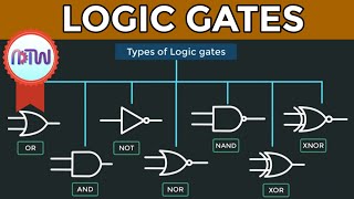
- This video is on basic logic gate timing diagram. AND logic gate output timing diagram is drawn when both the input timing diagram is given. The timing diagram of both the input A and B are applied as input to AND gate. The output timing diagram of F is drawn for inputs.


Thank you so much ma'am I've breaking my head for a while on how to solve these types of problems. You just gained a new subscriber!!
🙏
Very very clear to understand
Glad it helped
I find it helpful, Thanks
Glad you like it.
Clearly understood! Thank u mam 😊
Glad you like it. Please subscribe my channel to support us.
Nice video mam...
Thank you.
aunty thank you
Madam tq very much
Hm ny yh mid mein q line lambi ki?
Dono me se agar ek bhi input zero hai to output zero hoga. Second input mid me zero hain isliye mid me line zero hain.
Hindi 🤔😡