If you are in Auckland you should ask if you can get a tour. Richard has given our company a few tours of the workshop. Its cooler to see in person, and you get to ask all the questions! He's a nice guy, very helpful.
The reason they electroplated the copper the second time was to increase the copper up to the required thickness. The copperclad they use only has a thin layer of copper on it. That allows them to etch them faster and have finer traces.
IIRC, it is a palladium based chemical, that deposits electroless extremely thin layer, this makes it conductive enough for electrolysis copper to deposit.
Nothing looked out of the ordinary for doing Dave's run then would be for a larger run. I assume this batch was for about 100-200 uCurrents or so. None of the process seemed to be set up just for him other then v-scoring. I too was susprised by all the manual labor. Seemed as if there was a good 15 mins of human time for each panel, if not more.
It's a small production run, so it wouldn't be really feasible considering variety of board sizes, special requirements and so on the PCB manufacturer has to cope with. If you deal with manufacturing BIG batches of few PCB types (like you make PCBs for PC motherboards) then of course line would be nearly fully automated - kind of factory where bare copper board comes one side, and trucks loaded with PCBs comes out another side;)
Yeah, but I thought there were circuit printers and they just apply a layer of whatever. Then send through the conductive printer again. Repeat as needed.
Of the hundreds of your videos that I have watched Dave, that was the bees knees mate! Thankyou for all the time and effort you put into your superb videos :) Much love from the UK!
How can someone Thumbs Down this easy to understand informative Video ??? It must no doubt be over their tiny little heads. Yeah the costs have come drastically down since I had my 1st prototype professional PCBs made. The 10pc 2" X 3" double sided PCBs cost me near $400 Cnd about 30 years ago. Today I can get the same PCBs made for less than $2.00 each delivered... from China
This process seems to be tiny compared to what I do every day at work. We make multi layer panels and start off with inner layer cores that are etched, punched, scanned (I am an AOI scanner), lay up, press, flash, then drill. And the electroless lines at my work are massive, the panels are carried by a massive crane from tank to tank. Theses panels are also very small, the panels we process can be as big as 36x34 inches down to 18x24 inches. You didn't get to show the full process sadly, but it's nice to see a process shown online.
Indeed. The CNC drilling machine shown seems to be a 1985...1990 model, having two 5-1/4'' floppy drives and a paper tape punch unit. Larger factories will use faster, much modern equipment, for sure.
Card edge connectors are hard gold which is a galvanic process. You pay a premium for combining the normal chem. NiAu for SMD and the galvanic Hard Gold for the card edge connector. This is important as you should not solder on Hard Gold, as Gold easily alloys with tin, forming a bridle joint.
Yes, correct, should have mentioned that. Although if you only need a few insertions for a test connector or something, regular electroless gold edge connectors are just fine.
the chemicals, the machinery, the manpower, the design hours, the gas and coffee for all people involved, the metal, the expertise, the overhead. Its not cheap, yo.
Wow, the CNC electrical continuity tester is one I never thought of. Amazing. All of the processes are amazing. Something to work towards. Excellent video.
10:42 I have heard from some manufacturers that they have a rather thin base layer of copper, and by electrolysis they deposit the amount of copper required for the desired thickness. That way when there is the etching step, there is only the thin layer of copper to be etched away. I was really hoping to see more on how the through hole plating works, its still not totally clear for me and my home brew process is quite lacking....
tjeulink I know very well how it works, but for the holes, I wanted more details, as the professional ones have very controlled uniform thickness which I was never able to achieve at home, so the question here is what they do differntly (other than probably higher current, I don't think thats the only difference)
tjeulink I am stirring/pumping the mixture too (which you should to avoid any posibly ocurring bubbles to be removed as soon as possible). It might also be a chemical thing, as depending on various parameters the deposited surface changes in quality. There is a lot of trial and error and company secrets involved in getting it right
Stefan Santiago No wonder Chinese boards cost a dollar (sometimes 1/2 dollar) for 100mmx100mm 2 side, with top silk, each. And they are pretty good boards, same thing made in USA, $25 each. I feel really bad, but USA is not a good place for competing with asian board houses. Most are gone now.
I am surprised at how much manual labor goes in to this. I thought the reason you could get PCB production so cheap these days was that it had become highly automated.
MrCravon I've been working on the inner layers portion of a PCB process and I can tell you a lot of stuff requires that human touch, picky machines and loading them correctly is something tough for some robots.
+TheBoxxWillRuleAll Really, I too thought the boards would roll into an assembly line (similar to the development one in this video), and be mechanically constrained by side rollers combined with optical front edge detection for steps needing positional precision. I agree that arm-style robots wouldn't provide the precision, hence my idea that mechanical constraints and optical sensors would be used.
Actually, that would be a great video idea for Dave!!!! How could that not make a great video? Specifically if you ordered boards from a long list of prototype houses, get them in and then looked at them under a microscope for registration, errors, etc. Also compare real world cost, time to deliver, adherence to design rules, and maybe sneak in some parts of the PCB that violate it, to see what they do. All that good stuff. "No point" - meh. My only thing would be have them delivered to a person in the US. Why, cause Dave's audience is like 90% US based.
This is fascinating! Why anyone would down-vote resists explanation. The only part that I didn't follow was the thru-hole plating. How does the metal build up in the thru-holes?
As Ivan mentioned elsewhere in the thread, through holes can have metal chemically deposited using a palladium process. Once a base layer is there, copper can be electroplated on using a more traditional process.
Thanks for making this video. I have been looking for something like this for a couple of years, but have always only found how are PCBs being populated with components.
We actually do the film process in my Schools clean room.... mainly cause most of this equipment is insanely expensive and places have donated all the equipment. Its still very cool way of learning the manufacturing process and working in a clean room
The machine used to make the film for the photolithography is called an imagesetter. It's the same type of machine used for making masks for photoetching of printing plates, and once used to make semiconductor photomasks as well.
As someone who's done some basic screen printing, it's really interesting to me how they print over an entire board and expose the "paint" instead of exposing an emulsion on the screen.
I think it is much faster to coat the whole board and use that masking to do the wanted image. Yeah, it wastes the ink but the other process wastes the holy silk screen.
As a Texan, I'm surprisingly amused by your Australian euphemisms. The "How you doin'" and "Bobs' your uncle" completely elude me as to their origin, but I'm determined to find out! I just figured out who this "Bobby Dezzla (Dazzler)" fella is..... Great video as always. This is very informative. I watched a video on how to do PCBs at home, but sending it off seems the proper way to get it done. Still, it's a fun home project once or twice.
Thanks Dave for this video! Very informative and accurate! However, I'll suggest that you should do a video on how to do your own PCB's at home. I started that way many years ago and it made me a better PCB designer since a I'm able to better understand what is the fabrication process and it's limitations. Even though you do not have plated thru hole on a home PCB, it is possible to design the board by taking that into account and avoiding top pad connection underneat capacitors, connectors and IC's and using vias instead. When I'm doing my own PCB, I'm using the toner transfer from a laser printer onto bare pcb boards and it's surprisingly alot better than the photo imaging process that I was using 15 years ago. It is a lot less expensive and the failure rate is really low. I can easily etch traces down to 10 mils using toner transfer!
The PCB is made of glass fiber cloth layers sandwiched together with a layer of copper sheet on one (or both) sides all glued together with epoxy under pressure. Once you have a fiberglass and copper sheet, the rest of the process in this video is executed.
I used to work in a PCB factory when I was a kid and it is quite simple. The design is laid out and and through photo-lithography a negative is exposed onto double sided copper coated fiberglass so that the only thing showing are the traces and holes which are drilled automatically after the photo-lithography. The boards are then attached to "trees" and washed in a mild acid bath. From there is goes into a copper-sulfate bath and electroplated where only the exposed areas of the large board (which may contain many duplicates of the same small board) is plated. When it's done, the thickness is checked on several parts of the board to make sure the electroplating was even and built up to the right thickness. At this point, the boards are still 100% covered with copper, but most of the board has a blue photoresist layer on it so that only the traces are exposed. Then they are washed again in a mild acid bath. From there they get plated with tin-lead, so that all exposed areas of the board (mostly traces and ground planes) are covered in tin-lead. Then, the trees are transferred into an acid bath which removes the photoresist layer from the board. Then the trees are put into an etching bath that dissolves all the exposed copper. The trees are then moved once again into a a mild acid cleaning bath. Then they are put into yet another bath witch removes the tin-lead layer. This is all done by hand. The trees are picked up and transferred to the various baths and screwed onto large bars at the top of the baths. The bars act to hold the trees (which the boards are clamped to) and the trees are fully conductive from the bars and the boars are slightly larger than the total used space so that the trees are always in full electrical contact with the boards. If there are any gold-plated card edge connectors on the boards, they go through the same process, but this is done mostly by hand (on a small scale) because you only want to gold plate what needs to be gold plated. After this, the boards are shipped to a another factory that can do the pick and place. The place I worked for did mostly low volume, but very high quality industrial boards. I remember one of the main customers was an automobile shop diagnostic equipment manufacturer (this was like 25 years ago, but I want to say Bear was a big customer). They no longer exist. They use a lot of chemicals and once in a while will accidentally created a bunch of chlorine gas. The copper plating using "copper nuggets" which are essentially 1" thick extruded bars cut every 1.5". The tin-lead plating used solid bars of tin-lead. Sulfuric acid was heavily used as well as some much milder acids. There is constant cleaning of the boards and you always have to wear gloves to keep your skin and oil off the boards (and to protect your own hands from all these chemicals). This is old tech, but there really wasn't anything especially complicated about it. Chemists would periodically take samples from the various baths and concentrate or distilled water would be added as needed.
11:20 are you sure that they cover traces with tin before etching copper? The tin will melt in reflow oven right under the solder mask and the solder mask will peel off.
Considering the price I'm amazed at how much work goes into making a board, especially how much of the work is manually loading the boards. For the price you pay I'd have expected a lot more automation.
Highly automated plants want to make high (profit) margin boards, and typically have their production capacity tied up doing so. Small run prototype work typically goes to the small shops.
12:15 No Dave, what they are doing is exactly how this was done when I worked in a PCB factory (like 1990). They even use similar trees. This was always done with negative photo-lithography. TBH, I'm quite surprised that this hasn't really changed at all. The only difference I can see so far is that this facility is setup for smaller board runs. It's a shame you probably don't have any gold plating on your board (for card edge connectors). It's done much more efficiently so you don't lose any of the gold. They also keep the card edge connector/gold plating stuff under lock and key. People used to steal the copper nuggets, but they really weren't worth much, but gold is. I never even saw one because I had no access to the gold plating department.
The bare panel has maybe 0.25oz copper on it. So they photo-plot the negative, so they can build up the thickness on the traces to the desired thickness. Then they etch off the unwanted copper. This minimizes under-cut during the etching process.
The film imaging engine is an Agfa SelectSet 7000 imagesetter. It has the capability of imaging 1200, 2400 or 3600 dpi on film up to 25.6 inches wide. I used one about 20 years ago in a printing pre-press shop.
10:40 This is the actual plating that builds up the traces and the ground plate. If you didn't do this step, your traces would only be as thick as the copper coating on the fiberglass board. To keep costs of the boards down, the copper coating is extremely thin. Where I worked, this particular process took like 45 minutes. That is a copper-sulfate bath with a copper source in it. Where I worked they used these long thin "baskets" filled with copper nuggets.
OSHPark rocks! I used to etch my own PCBs since I was 10 (ah, the ferric chloride stains in the bathroom sink. My Mom just "loved" me for it...), but now, there's no point in making a mess.
You can do a simple silkscreen on your homemade DIY boards by toner transferring it on after etching. Pretty much essential if you have over 50 components.
Yea, there is another step there that was left out. I think there is some conductive material(goo) that is put into the edges of the holes, that allow the holes to be plated. That was kinda of a head scratcher for me too. Wish Dave had addressed it. Maybe he forgot. It's not like him to shy away from love detailed videos!
I know 4pcb uses an chemical electroless processe to putt a few microns of copper down on the bare fr4 in the holes then they electroplate to the final copper thickness
I always wondered how this was done. My home brew "vias" are just chopped off bits of resistor leads soldered and trimmed in place. I still don't understand how its is through plated, and blind vias are another enigma. Also, 4,6,8+ layer PCB from 2 double sides makes sense, but what is used to isolate the layers, just soldermask?
With blind vias, the inner layers are drilled and run through the electroless process before lamination. We charge extra for buried vias. (In the particular process I worked with.)
You use the electroplating after film development to be more efficient in the use of the copper. The base board has only a thin copper layer of 1µm or less. On the exposed parts the copper is electroplated to the desired thickness. Afterwards you only have to etch away the thin base plating which is faster and consumes less copper in total. You could even skip the tin-plating step here: eletroplating to a thickness of 18µm and then etching away 1µm of copper over the whole board will consume all copper between the traces, but the thickness of the traces would only be reduced by 1µm to the standard 17µm. No risk of underetching here as well - yet another advantage of this method.
What do they do differently for small production runs (like prototype boards)? The router seems like the slower part of the process, how do they deal with boards that have a few billion vias? Are small vias processed any differently than your larger plated through-hole?
While drilling small holes, Excellon CNC may work as fast as 1...2 hits per second (depending on board size, average distance and path optimization between holes). To drill 0,9mm holes, the spinners are set to 65,000RPM and the Z (vertical) feed speed is set near maximum. When drilling larger holes (screw mounting ones, etc.), spinners are set to 20,000...25,000RPM at lower Z feed speed. In a recent job, our Excellon 3-head machine spent about 12 minutes to execute 1370 0,9mm hits in a non-typical board (holes very close to each other) -- 1.9 hits per second average speed. Grouping 3-board height stacks, the rate is 17 holes per second. Altough a typical board drilling will be a bit slower, this is fast, indeed.
Jackson Gray usually machines can drill about 30,000 holes per hour, if they are less than 6 mil they may laser drill them. Some machines are faster then others but drilling is very time consuming.
Jackson Gray for the billion vias some mfg houses use laser cnc instead of mechanical drilling. When you see via capabilities of ungodly tinyness, you know they're using laser. Faster drilling and even arbitrary diameter holes.
Thx, Dave. Thumbs up! Simple, not overloaded video about bad to health work. Don't you whant to make a video about 4-layer board tracing basics? For example, with 2 external signal layers and 2 internal power layers.
Very nice Dave. Thank you! I love seeing these kind of videos :) Hope to order boards for my Tron Identity Disk project soon. Will be using the Elektor print service (Eurocircuits).
I wonder if they even do this in America still. This is a labor intensive and is virtually unchanged since I was working in a PCB factory in 1990. The way we did this stuff, when the electroplating was happening, you mostly just sat there and waited for the thing to finish. Sometimes, when we were busy, we would load the trees, but that was only if we had the spare trees and the very first tank, which was a weak acid/water mix, was free. We spent a good portion of the day just waiting for the electroplating to finish. It's usually about an hour. You move the trees from the copper to the tin-lead, give the ones in the tin lead to the next guy, move the ones from the cleaning bath to the copper bath and load the water/acid bath and all this only takes about 15 minutes, so you really just sit around or clean or other make-work for 30-45 minutes (the specs determine how long the main copper bath lasts, usually about 1 hour). Moving those trees around was hard work and you had to wear these large rubber aprons and there was no air-conditioning. It hurt your back and you sweat your ass off. The environmental people would show up all hours of the day and night for spot checks. The floor was a "board walk" All the wiring for the DC current used for the machines were under the board walk and it also kept the floor dry from constantly moving the trees from one bath to the next. The liquids would pour off the boards when took the trees out to move them to the next process and there would have been puddles of acids on the floor without that "board walk" design..
Hi Dave, the older videos you talked about are not clickable, also no links for them in the description (e.g. 2:15). Anyway, great video as usual. Thanks !
One of the reasons the panel is bigger is for the tree to connect to the panel while maintaining electrical continuity. If they weren't bigger, the trees would NOT conduct electricity through the photoresist mask during the electroplating portion of manufacturing your board.
How can you go round this place and decide not to upload the footage straight away or within a few weeks at least? Makes me wonder what else is stored on that computer. Very interesting though. So thankyou
Usually these bare Panels have 17.5µm copper so the etching solution wont be saturated that fast to reduce cost. Also etching will work significantly faster AND the possibility of over- and under etching will be reduced. :) At 11:00 they put it back in the copper electrolysis bath to add the copper to get the standard 35µm thickness (I guess you've specified 35µm. :)).
Dave, in the video you mentioned that Electoless gold (ENIG) is really great for high pin count chips due to the flatness and low cost adder. This is something I've been researching recently and also been finding to be true. If it is so good and relatively cheap, why do so many other plating types exist? HASL, Organic, Tin Immersion, Silver Immersion, ENIG, etc? I've not found any compelling arguments for when and why you would choose the other finishes. If you have any insights, I would love to hear them.
Gold plating for mechanical scratch resistance on exposed pads (like contact points on PCI or memory cards) and corrosion prevention. Most expensive. 2. Silver plating for Corrosion prevention, surface planarity, solder adhesion. Cheaper than gold. 3. Tin plating for solder adhesion. But no corrosion prevention. Cheaper than silver. 4. HASL is the coating of copper with molten solder by dipping in molten solder bath and then removing the excess with hot air. Excellent solderability can be achieved, but surface planarity is not as good as silver or gold. 5. Organic coating is a temporary protection applied to exposed copper or tin plated PCBs to prevent oxidation or corrosion during storage before soldering.
I'm trying to make simple LDI with laser module from a laser printer. Still far from success - currently I'm fighting with PLL for laser synchronization, but the amount of things I learned during that - priceless.
I think I got the reason for negative photo resist masking for the copper layer - tinning. That is the only way they can electroplate the tin on the copper layer in one go. If they use positive photo resist and a total cover of tin, then they will have to apply tin before the mask and then they will have to do a dual etching of tin first and copper later. If they do copper etching first, then they have to electroplate tin trace by trace as there needs an electric connection between the copper and the plating solution.
I think they pattern-plate (tin-plate) the design before etching so the etchant doesn't get into your vias and cause problems. I'm not sure how you'd be able to protect the vias with etch-resist otherwise.
Hey Dave, nice video! do you happen to know what kind of ink they use for the soldermask and silkscreen? I've been searching for those like crazy, thanks man!
How are those sheets not sticking to the ink when he places them on the fresh uv ink to be exposed, @ 13:05 and 15:25 ? it looks like they are already cured because they don't stick. this is where I always make a mess with my boards. anybody know what's going on there?
Great vid, I could watch stuff like this all day! I'm left with one question though, why would you rout out the panel when you're going to snap the boards out anyways? I can't remember your test jig, but did it register off the panel outer edges? I'd be aiming to reuse the manufacturers pin holes.
Theres lots of people doing through hole with soldermask and liquid tin at home. As long as you have a decent cnc machine or laser printer your good to go. Its great for prototyping and then when you got finished it send it off.


That was really interesting. It was good of them to shoot the video for you and they actually did a decent job of it.
If you are in Auckland you should ask if you can get a tour. Richard has given our company a few tours of the workshop. Its cooler to see in person, and you get to ask all the questions! He's a nice guy, very helpful.
The reason they electroplated the copper the second time was to increase the copper up to the required thickness. The copperclad they use only has a thin layer of copper on it. That allows them to etch them faster and have finer traces.
Because you can't elecrolytically grow copper on non-conductive surface. They use something to grow copper inside plated holes, not sure what exactly.
IIRC, it is a palladium based chemical, that deposits electroless extremely thin layer, this makes it conductive enough for electrolysis copper to deposit.
And it guarantees that the through hole plating connects to the surface plating.
it's easier to plate up to the required thickness, than to etch down to the specified thickness
I'm really surprised that most of this isn't automated completely.
in smaller factories this is not that uncommon i think, plus its a lot more flexible if you have a human there.
Nathan Trone i think that is because these are prototypes.
Nothing looked out of the ordinary for doing Dave's run then would be for a larger run. I assume this batch was for about 100-200 uCurrents or so. None of the process seemed to be set up just for him other then v-scoring. I too was susprised by all the manual labor. Seemed as if there was a good 15 mins of human time for each panel, if not more.
It's a small production run, so it wouldn't be really feasible considering variety of board sizes, special requirements and so on the PCB manufacturer has to cope with. If you deal with manufacturing BIG batches of few PCB types (like you make PCBs for PC motherboards) then of course line would be nearly fully automated - kind of factory where bare copper board comes one side, and trucks loaded with PCBs comes out another side;)
Yeah, but I thought there were circuit printers and they just apply a layer of whatever. Then send through the conductive printer again. Repeat as needed.
Of the hundreds of your videos that I have watched Dave, that was the bees knees mate!
Thankyou for all the time and effort you put into your superb videos :)
Much love from the UK!
Wow, pcb manufacture is an incredible process. So time consuming and repetitive and complex. Very good to see, thanks Dave.
How can someone Thumbs Down this easy to understand informative Video ???
It must no doubt be over their tiny little heads.
Yeah the costs have come drastically down since I had my 1st prototype professional PCBs made. The 10pc 2" X 3" double sided PCBs cost me near $400 Cnd about 30 years ago. Today I can get the same PCBs made for less than $2.00 each delivered... from China
This process seems to be tiny compared to what I do every day at work. We make multi layer panels and start off with inner layer cores that are etched, punched, scanned (I am an AOI scanner), lay up, press, flash, then drill. And the electroless lines at my work are massive, the panels are carried by a massive crane from tank to tank. Theses panels are also very small, the panels we process can be as big as 36x34 inches down to 18x24 inches. You didn't get to show the full process sadly, but it's nice to see a process shown online.
Yeah, this is a very small scale facility.
Indeed. The CNC drilling machine shown seems to be a 1985...1990 model, having two 5-1/4'' floppy drives and a paper tape punch unit. Larger factories will use faster, much modern equipment, for sure.
please make a video
Thanks for adding the design and hard edge video links Dave, was confused until I refreshed :)
Great video Dave - especially given that it is your PCB in the videos.
Card edge connectors are hard gold which is a galvanic process. You pay a premium for combining the normal chem. NiAu for SMD and the galvanic Hard Gold for the card edge connector. This is important as you should not solder on Hard Gold, as Gold easily alloys with tin, forming a bridle joint.
Yes, correct, should have mentioned that. Although if you only need a few insertions for a test connector or something, regular electroless gold edge connectors are just fine.
che?
Dave your video was a blessing is disguise to me yesterday evening! I got to learn some info, and it cured my sleeplessness ;)
They are very inexpensive to produce. This was one of the better videos that I've seen showing the entire process.
the chemicals, the machinery, the manpower, the design hours, the gas and coffee for all people involved, the metal, the expertise, the overhead. Its not cheap, yo.
the infinite number of steps. im only on minute 26 of this video
Wow, the CNC electrical continuity tester is one I never thought of. Amazing. All of the processes are amazing. Something to work towards. Excellent video.
Really interesting to see this entire process - also it's ridiculous how much manual work still goes into this!
I really enjoyed this video. Quite interesting what processes are used and in what order they are done. Thanks for sharing it with us!
10:42 I have heard from some manufacturers that they have a rather thin base layer of copper, and by electrolysis they deposit the amount of copper required for the desired thickness. That way when there is the etching step, there is only the thin layer of copper to be etched away.
I was really hoping to see more on how the through hole plating works, its still not totally clear for me and my home brew process is quite lacking....
Dennis Lubert look up how electrolysis works, that probably helps you understand it :)
tjeulink I know very well how it works, but for the holes, I wanted more details, as the professional ones have very controlled uniform thickness which I was never able to achieve at home, so the question here is what they do differntly (other than probably higher current, I don't think thats the only difference)
Dennis Lubert hmm interesting, maybe they pump around the mixture or jet it directly on the pcb?
tjeulink I am stirring/pumping the mixture too (which you should to avoid any posibly ocurring bubbles to be removed as soon as possible). It might also be a chemical thing, as depending on various parameters the deposited surface changes in quality. There is a lot of trial and error and company secrets involved in getting it right
Yea.. it seams to be the case. This way they can use far less copper as well. The original layer can be really really thin.
Damn that's a lot of work....
2/10 needs more automation and more clean.
Brad The PCB manufacturing process is very automated, and unfortunately very messy, no way around that.
Stefan Santiago
No wonder Chinese boards cost a dollar (sometimes 1/2 dollar) for 100mmx100mm 2 side, with top silk, each. And they are pretty good boards, same thing made in USA, $25 each. I feel really bad, but USA is not a good place for competing with asian board houses. Most are gone now.
I am surprised at how much manual labor goes in to this. I thought the reason you could get PCB production so cheap these days was that it had become highly automated.
MrCravon I've been working on the inner layers portion of a PCB process and I can tell you a lot of stuff requires that human touch, picky machines and loading them correctly is something tough for some robots.
+TheBoxxWillRuleAll Really, I too thought the boards would roll into an assembly line (similar to the development one in this video), and be mechanically constrained by side rollers combined with optical front edge detection for steps needing positional precision. I agree that arm-style robots wouldn't provide the precision, hence my idea that mechanical constraints and optical sensors would be used.
On minimum wage
the technology hasn't become automated, it has just moved to china
You should send your board files to cheaper "hobbyist" type PCB fabs like pcbway, dirtypcbs and elecrow to compare the results. That would be neat.
No point
Actually, that would be a great video idea for Dave!!!! How could that not make a great video? Specifically if you ordered boards from a long list of prototype houses, get them in and then looked at them under a microscope for registration, errors, etc. Also compare real world cost, time to deliver, adherence to design rules, and maybe sneak in some parts of the PCB that violate it, to see what they do. All that good stuff. "No point" - meh. My only thing would be have them delivered to a person in the US. Why, cause Dave's audience is like 90% US based.
Thats what PCB Shopper is for :)
Plus...the quality varies week to week. Its really just luck of the draw
He has compared a couple of the hobbyist PCB fabs in the past, iTead vs another i cant remember the name of.
+GeorgeGraves Err, no, less than 30% of my audience is from the US. Yes it's my largest segment, but still only less than a 1/3rd
This is fascinating! Why anyone would down-vote resists explanation. The only part that I didn't follow was the thru-hole plating. How does the metal build up in the thru-holes?
I guess it's always the batterizer people that down-vote; they're traumatized by Dave debunking their bullshit ;)
As Ivan mentioned elsewhere in the thread, through holes can have metal chemically deposited using a palladium process. Once a base layer is there, copper can be electroplated on using a more traditional process.
Either electroless copper or direct metalisation process which is fundamental but not shown
This is a very interesting process. It'll be great if you could make a video showing the complete updated process for comparison.
I wonder how many more amazing videos like this one are 'waiting to be edited'. I bet a lot of those will never see the light of day. Ts, ts, ts...
was waiting a long time for such a video again(Back to the basics) well done , love it
Fascinating! I love episodes that give us a peek into the world of electronics manufacture!
Thanks for making this video. I have been looking for something like this for a couple of years, but have always only found how are PCBs being populated with components.
We actually do the film process in my Schools clean room.... mainly cause most of this equipment is insanely expensive and places have donated all the equipment. Its still very cool way of learning the manufacturing process and working in a clean room
Developer! Developer! Developer! Developer!
Oh, Hi Steve!
The machine used to make the film for the photolithography is called an imagesetter. It's the same type of machine used for making masks for photoetching of printing plates, and once used to make semiconductor photomasks as well.
One of the most interesting videos I've seen recently, time flew very fast.
Interesting to see how different companies do this.
As someone who's done some basic screen printing, it's really interesting to me how they print over an entire board and expose the "paint" instead of exposing an emulsion on the screen.
I think it is much faster to coat the whole board and use that masking to do the wanted image. Yeah, it wastes the ink but the other process wastes the holy silk screen.
As a Texan, I'm surprisingly amused by your Australian euphemisms. The "How you doin'" and "Bobs' your uncle" completely elude me as to their origin, but I'm determined to find out! I just figured out who this "Bobby Dezzla (Dazzler)" fella is..... Great video as always. This is very informative. I watched a video on how to do PCBs at home, but sending it off seems the proper way to get it done. Still, it's a fun home project once or twice.
Good video. Loved it. Roller/HAL tinning is still done by many, though, it seems.
Thanks Dave for this video! Very informative and accurate! However, I'll suggest that you should do a video on how to do your own PCB's at home. I started that way many years ago and it made me a better PCB designer since a I'm able to better understand what is the fabrication process and it's limitations.
Even though you do not have plated thru hole on a home PCB, it is possible to design the board by taking that into account and avoiding top pad connection underneat capacitors, connectors and IC's and using vias instead.
When I'm doing my own PCB, I'm using the toner transfer from a laser printer onto bare pcb boards and it's surprisingly alot better than the photo imaging process that I was using 15 years ago. It is a lot less expensive and the failure rate is really low. I can easily etch traces down to 10 mils using toner transfer!
Very informative video Dave, thanks!
My old job - CNC drilling. The boards i used to drill were normally pinned in 3's. An old cassette tape media for the CNC program.
Wonderful video to watch, very informative!
Awesome! Full of data and demo!
This was a great video. Thanks Dave!
how is pcbb formed
*pregananant
its like birth, when an fr4 loves an etchant.....
*pregnant
r u 12
The PCB is made of glass fiber cloth layers sandwiched together with a layer of copper sheet on one (or both) sides all glued together with epoxy under pressure. Once you have a fiberglass and copper sheet, the rest of the process in this video is executed.
Exactly I wonder whats going on with non plated holes, and get the conclusion like explanation here - thanks!
I used to work in a PCB factory when I was a kid and it is quite simple.
The design is laid out and and through photo-lithography a negative is exposed onto double sided copper coated fiberglass so that the only thing showing are the traces and holes which are drilled automatically after the photo-lithography. The boards are then attached to "trees" and washed in a mild acid bath. From there is goes into a copper-sulfate bath and electroplated where only the exposed areas of the large board (which may contain many duplicates of the same small board) is plated. When it's done, the thickness is checked on several parts of the board to make sure the electroplating was even and built up to the right thickness. At this point, the boards are still 100% covered with copper, but most of the board has a blue photoresist layer on it so that only the traces are exposed. Then they are washed again in a mild acid bath. From there they get plated with tin-lead, so that all exposed areas of the board (mostly traces and ground planes) are covered in tin-lead. Then, the trees are transferred into an acid bath which removes the photoresist layer from the board. Then the trees are put into an etching bath that dissolves all the exposed copper. The trees are then moved once again into a a mild acid cleaning bath. Then they are put into yet another bath witch removes the tin-lead layer. This is all done by hand. The trees are picked up and transferred to the various baths and screwed onto large bars at the top of the baths. The bars act to hold the trees (which the boards are clamped to) and the trees are fully conductive from the bars and the boars are slightly larger than the total used space so that the trees are always in full electrical contact with the boards. If there are any gold-plated card edge connectors on the boards, they go through the same process, but this is done mostly by hand (on a small scale) because you only want to gold plate what needs to be gold plated. After this, the boards are shipped to a another factory that can do the pick and place. The place I worked for did mostly low volume, but very high quality industrial boards. I remember one of the main customers was an automobile shop diagnostic equipment manufacturer (this was like 25 years ago, but I want to say Bear was a big customer). They no longer exist. They use a lot of chemicals and once in a while will accidentally created a bunch of chlorine gas. The copper plating using "copper nuggets" which are essentially 1" thick extruded bars cut every 1.5". The tin-lead plating used solid bars of tin-lead. Sulfuric acid was heavily used as well as some much milder acids. There is constant cleaning of the boards and you always have to wear gloves to keep your skin and oil off the boards (and to protect your own hands from all these chemicals). This is old tech, but there really wasn't anything especially complicated about it. Chemists would periodically take samples from the various baths and concentrate or distilled water would be added as needed.
I honestly wasn't expecting it to be that much work, very impressive. I'll never complain about the price of a high-end motherboard again.. :)
11:20 are you sure that they cover traces with tin before etching copper? The tin will melt in reflow oven right under the solder mask and the solder mask will peel off.
Considering the price I'm amazed at how much work goes into making a board, especially how much of the work is manually loading the boards. For the price you pay I'd have expected a lot more automation.
Highly automated plants want to make high (profit) margin boards, and typically have their production capacity tied up doing so. Small run prototype work typically goes to the small shops.
Cool vid Dave. Would love if you could do one called 'EEVBOG #1000 How Is An IC Manufactured?'
That was very interesting and fun to watch!
Very interesting! Thanks, Dave!
Wow that is an interesting process. I compare that to a home made and home etched PCB and there just is no comparison. Nice one Dave.
12:15 No Dave, what they are doing is exactly how this was done when I worked in a PCB factory (like 1990). They even use similar trees. This was always done with negative photo-lithography. TBH, I'm quite surprised that this hasn't really changed at all. The only difference I can see so far is that this facility is setup for smaller board runs. It's a shame you probably don't have any gold plating on your board (for card edge connectors). It's done much more efficiently so you don't lose any of the gold. They also keep the card edge connector/gold plating stuff under lock and key. People used to steal the copper nuggets, but they really weren't worth much, but gold is. I never even saw one because I had no access to the gold plating department.
The bare panel has maybe 0.25oz copper on it. So they photo-plot the negative, so they can build up the thickness on the traces to the desired thickness. Then they etch off the unwanted copper. This minimizes under-cut during the etching process.
I use to work in a PCB factory - I printed the ident layers -AMA!
The film imaging engine is an Agfa SelectSet 7000 imagesetter. It has the capability of imaging 1200, 2400 or 3600 dpi on film up to 25.6 inches wide. I used one about 20 years ago in a printing pre-press shop.
10:40 This is the actual plating that builds up the traces and the ground plate. If you didn't do this step, your traces would only be as thick as the copper coating on the fiberglass board. To keep costs of the boards down, the copper coating is extremely thin. Where I worked, this particular process took like 45 minutes. That is a copper-sulfate bath with a copper source in it. Where I worked they used these long thin "baskets" filled with copper nuggets.
OSHPark rocks!
I used to etch my own PCBs since I was 10 (ah, the ferric chloride stains in the bathroom sink. My Mom just "loved" me for it...), but now, there's no point in making a mess.
You can do a simple silkscreen on your homemade DIY boards by toner transferring it on after etching. Pretty much essential if you have over 50 components.
How does the electrolysis bath plate the holes? Aren't the holes just naked glass fiber and resin?
Yea, there is another step there that was left out. I think there is some conductive material(goo) that is put into the edges of the holes, that allow the holes to be plated. That was kinda of a head scratcher for me too. Wish Dave had addressed it. Maybe he forgot. It's not like him to shy away from love detailed videos!
I know 4pcb uses an chemical electroless processe to putt a few microns of copper down on the bare fr4 in the holes then they electroplate to the final copper thickness
I always wondered how this was done. My home brew "vias" are just chopped off bits of resistor leads soldered and trimmed in place. I still don't understand how its is through plated, and blind vias are another enigma.
Also, 4,6,8+ layer PCB from 2 double sides makes sense, but what is used to isolate the layers, just soldermask?
With blind vias, the inner layers are drilled and run through the electroless process before lamination. We charge extra for buried vias. (In the particular process I worked with.)
You had this footage for 4 years?
You use the electroplating after film development to be more efficient in the use of the copper. The base board has only a thin copper layer of 1µm or less. On the exposed parts the copper is electroplated to the desired thickness. Afterwards you only have to etch away the thin base plating which is faster and consumes less copper in total. You could even skip the tin-plating step here: eletroplating to a thickness of 18µm and then etching away 1µm of copper over the whole board will consume all copper between the traces, but the thickness of the traces would only be reduced by 1µm to the standard 17µm. No risk of underetching here as well - yet another advantage of this method.
Hopefully, we'll be 3d printing them some day.
What do they do differently for small production runs (like prototype boards)? The router seems like the slower part of the process, how do they deal with boards that have a few billion vias? Are small vias processed any differently than your larger plated through-hole?
Vias are no different to any through-hole pad. Proto panels will often have limits on how many holes you can have for that low cost.
While drilling small holes, Excellon CNC may work as fast as 1...2 hits per second (depending on board size, average distance and path optimization between holes). To drill 0,9mm holes, the spinners are set to 65,000RPM and the Z (vertical) feed speed is set near maximum. When drilling larger holes (screw mounting ones, etc.), spinners are set to 20,000...25,000RPM at lower Z feed speed.
In a recent job, our Excellon 3-head machine spent about 12 minutes to execute 1370 0,9mm hits in a non-typical board (holes very close to each other) -- 1.9 hits per second average speed. Grouping 3-board height stacks, the rate is 17 holes per second. Altough a typical board drilling will be a bit slower, this is fast, indeed.
Jackson Gray usually machines can drill about 30,000 holes per hour, if they are less than 6 mil they may laser drill them. Some machines are faster then others but drilling is very time consuming.
Jackson Gray for the billion vias some mfg houses use laser cnc instead of mechanical drilling. When you see via capabilities of ungodly tinyness, you know they're using laser. Faster drilling and even arbitrary diameter holes.
GOOD Stuff Dave! Awesome information. I used to "burn" mine on the patio. And every one of them sucked. LOLOL Life in 2017 is awesome.
Thx, Dave. Thumbs up! Simple, not overloaded video about bad to health work.
Don't you whant to make a video about 4-layer board tracing basics? For example, with 2 external signal layers and 2 internal power layers.
Very nice Dave. Thank you!
I love seeing these kind of videos :)
Hope to order boards for my Tron Identity Disk project soon.
Will be using the Elektor print service (Eurocircuits).
Just sent my gerbers off to PCBZone! Can't wait
excellent video. thank you Dave !!
For vias, would they drill out the hole and then plate it? Or is it more like a rivet that gets punched in?
I wonder if they even do this in America still. This is a labor intensive and is virtually unchanged since I was working in a PCB factory in 1990. The way we did this stuff, when the electroplating was happening, you mostly just sat there and waited for the thing to finish. Sometimes, when we were busy, we would load the trees, but that was only if we had the spare trees and the very first tank, which was a weak acid/water mix, was free. We spent a good portion of the day just waiting for the electroplating to finish. It's usually about an hour. You move the trees from the copper to the tin-lead, give the ones in the tin lead to the next guy, move the ones from the cleaning bath to the copper bath and load the water/acid bath and all this only takes about 15 minutes, so you really just sit around or clean or other make-work for 30-45 minutes (the specs determine how long the main copper bath lasts, usually about 1 hour). Moving those trees around was hard work and you had to wear these large rubber aprons and there was no air-conditioning. It hurt your back and you sweat your ass off. The environmental people would show up all hours of the day and night for spot checks. The floor was a "board walk" All the wiring for the DC current used for the machines were under the board walk and it also kept the floor dry from constantly moving the trees from one bath to the next. The liquids would pour off the boards when took the trees out to move them to the next process and there would have been puddles of acids on the floor without that "board walk" design..
That is absolutely amazing how all those processes can lead to a board so cheap.... Its unbelievable
Hi Dave, the older videos you talked about are not clickable, also no links for them in the description (e.g. 2:15).
Anyway, great video as usual. Thanks !
Yes, flash does not work on my machine at the moment so I can't add annotations
EEVblog Flash??? why not html5? flash is pretty dangerous nowdays, don't even have it installed myself
Even adobe is killing off flash if it hasn't by now, HTLM5 way safer and better performer.
Donald Holben
althoug html5 already has loads of vulnerability's, its still way more secure :P
This is brilliant. Thanks so mutch!
One of the reasons the panel is bigger is for the tree to connect to the panel while maintaining electrical continuity. If they weren't bigger, the trees would NOT conduct electricity through the photoresist mask during the electroplating portion of manufacturing your board.
Handling the boards and chemicals without gloves. Must be a high quality manufacturing facility...
How can you go round this place and decide not to upload the footage straight away or within a few weeks at least? Makes me wonder what else is stored on that computer. Very interesting though. So thankyou
one of my favorites!
There is a lot more handcraft going to this than I would have thought. I guess they use more automated process when you are doing bigger batch.
Thanks Dave!
Very interesting! :)
really informative David
ALWAYS do the automated electrical test. Whew. I learned that the hard way. :)
Interesting video in a long time :)
Hey Marty, is stripper solution a type of solution that makes it's living on a pole?
Hey Marty, welcome to the party.
At 10:52 they are most likely plating up the copper thickness to the require copper weight.
10:34 Wow this is in fact a brilliant idea. This may be why they get straight wires.
Usually these bare Panels have 17.5µm copper so the etching solution wont be saturated that fast to reduce cost.
Also etching will work significantly faster AND the possibility of over- and under etching will be reduced. :)
At 11:00 they put it back in the copper electrolysis bath to add the copper to get the standard 35µm thickness (I guess you've specified 35µm. :)).
From the looks of it, around 11:10 they've added more copper and increased the trace thickness (before the tinning process)
interesting to see the process
Dave, in the video you mentioned that Electoless gold (ENIG) is really great for high pin count chips due to the flatness and low cost adder. This is something I've been researching recently and also been finding to be true. If it is so good and relatively cheap, why do so many other plating types exist? HASL, Organic, Tin Immersion, Silver Immersion, ENIG, etc? I've not found any compelling arguments for when and why you would choose the other finishes. If you have any insights, I would love to hear them.
Gold plating for mechanical scratch resistance on exposed pads (like contact points on PCI or memory cards) and corrosion prevention. Most expensive.
2. Silver plating for Corrosion prevention, surface planarity, solder adhesion. Cheaper than gold.
3. Tin plating for solder adhesion. But no corrosion prevention. Cheaper than silver.
4. HASL is the coating of copper with molten solder by dipping in molten solder bath and then removing the excess with hot air. Excellent solderability can be achieved, but surface planarity is not as good as silver or gold.
5. Organic coating is a temporary protection applied to exposed copper or tin plated PCBs to prevent oxidation or corrosion during storage before soldering.
I'm trying to make simple LDI with laser module from a laser printer. Still far from success - currently I'm fighting with PLL for laser synchronization, but the amount of things I learned during that - priceless.
I think I got the reason for negative photo resist masking for the copper layer - tinning. That is the only way they can electroplate the tin on the copper layer in one go.
If they use positive photo resist and a total cover of tin, then they will have to apply tin before the mask and then they will have to do a dual etching of tin first and copper later.
If they do copper etching first, then they have to electroplate tin trace by trace as there needs an electric connection between the copper and the plating solution.
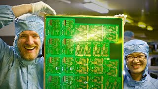
That's a gorgeous PCB !!!
I think they pattern-plate (tin-plate) the design before etching so the etchant doesn't get into your vias and cause problems. I'm not sure how you'd be able to protect the vias with etch-resist otherwise.
What are these traces in 23:47 ? the ones that look like antennas.
Hey Dave, nice video! do you happen to know what kind of ink they use for the soldermask and silkscreen? I've been searching for those like crazy, thanks man!
How are those sheets not sticking to the ink when he places them on the fresh uv ink to be exposed, @ 13:05 and 15:25 ? it looks like they are already cured because they don't stick. this is where I always make a mess with my boards. anybody know what's going on there?
Man, I really want to get some boards made now!
Do it!
Someone like PCBway (IIRC) shows you online the current processing step your boards are at.
I use Eurocircuits.
EEVblog Could you make a video with a comparison of some those cheap PCB manufacturers with respect to price and quality?
For my electronics project I got two quotes, one from pcbzone.net and one from JLCPCB.
One was 50x more expensive than the other.
Great vid, I could watch stuff like this all day!
I'm left with one question though, why would you rout out the panel when you're going to snap the boards out anyways?
I can't remember your test jig, but did it register off the panel outer edges? I'd be aiming to reuse the manufacturers pin holes.
Theres lots of people doing through hole with soldermask and liquid tin at home. As long as you have a decent cnc machine or laser printer your good to go. Its great for prototyping and then when you got finished it send it off.
21:07 Story of my life, paying per hole :/
I've never gotten a "flat rate for up to 300 holes" deal though.
11:37 i chose the stripper solution
Jordan Waeles Did you whack "it into the etchant"?
Pieh0 I think you'd need to use the etchant if you took the 300 holes deal.
Often they'll waive the fee if the drill size isn't too small.