PCB Plating Process | Multi-layer PCB Manufacturing Process - 06

HTML-код
- Опубликовано: 24 сен 2024
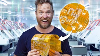
- To connect inter-layer circuits, the drilled boards must be plated. The first PCB plating process will be an electroless copper deposition procedure to coat a thin layer of copper on the surface of the board and into the drilled hole walls. And then the panel plating process is to increase the thickness of the copper layer.
Website:
www.pcbway.com
www.pcbway.es
www.pcbway.ru
www.pcbway.fr
www.pcbway.jp
Subscribe and follow us to keep updated with the latest news and promotion:
Facebook: / pcbway
Twitter: / pcbwayofficial
Instagram: / pcbway
VK: pcbway