Semiconductors & The Band Gap Structure Explained In 17 Minutes
HTML-код
- Опубликовано: 20 окт 2024
- Dr. Bedard(PhD) explains the evolution of semiconductors and the band gap structure that makes it all possible.
History of Semiconductors:
1) Early Observations: In the 19th century, Michael Faraday discovered that silver sulfide's conductivity increases with temperature, unlike metals.
2) Birth of Modern Semiconductors: In 1947, John Bardeen and Walter Brattain at Bell Labs developed the first point-contact transistor using germanium. In 1948, the junction transistor was invented, which became the basis for modern transistors.
3) Integrated Circuits: The late 1950s saw the development of the first integrated circuits, combining multiple transistors on a single substrate. Silicon became the preferred material due to its abundance, cost-effectiveness, and superior properties.
Basics of Semiconductors:
1) Electrical Conductivity: Semiconductors have conductivity between conductors (like metals) and insulators (like glass). Conductors allow free electron movement; insulators do not. Semiconductors' unique properties arise from their band structure.
2) Band Structure: The valence band is filled with electrons, and the conduction band is usually empty. The energy gap between these bands is the band gap.
3) Electron Movement: Electrons can jump from the valence to the conduction band, creating "holes" that act as positive charge carriers. Both electrons and holes contribute to electrical current.
Categories of Semiconductors & Doping:
1) Intrinsic Semiconductors: Pure semiconductors that behave like insulators at absolute zero. With temperature increase, some electrons move to the conduction band, allowing current flow.
2) Extrinsic Semiconductors: Doped with impurities to improve electrical properties. Doping creates P-type and N-type semiconductors.
-P-type: Doped with Group 13 elements (e.g., boron), creating holes.
-N-type: Doped with Group 15 elements (e.g., phosphorus), providing free electrons.
Creation of P-N Junctions:
1) Formation: When P-type and N-type materials join, they form a P-N junction. This allows current to flow in one direction (forward bias) and blocks it in the other (reverse bias).
2) Depletion Region: At the junction, electrons and holes recombine, creating a depletion region with no charge carriers, establishing an electric field.
Manufacturing of Semiconductor Devices:
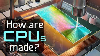
1) Process Overview: Involves wafer preparation, oxidation, photolithography, etching, ion implantation, deposition, planarization, and metallization.
2) Cleanliness: Semiconductor fabrication requires extremely clean environments to prevent defects and ensure high yields.
Semiconductor Components and Their Functions:
1) Diodes: Allow current to flow in one direction. Types include rectifier diodes (convert AC to DC), Zener diodes (voltage regulation), and LEDs (emit light).
2) Transistors: Amplify or switch electronic signals. Types include BJTs (current-controlled) and FETs (voltage-controlled).
3) Integrated Circuits (ICs): Miniaturized circuits combining multiple devices on a single chip. Used in both analog and digital applications.
Applications and Impact of Semiconductors:
1) Computing: Essential in CPUs, RAM, ROM, and GPUs. Semiconductors have enabled faster, more efficient processors and the miniaturization of electronic devices.
2) Real-World Impact: Advances in semiconductors have revolutionized computing, leading to high-speed computing, multitasking, and compact portable devices.
Future Trends in Semiconductor Technology:
1) New Materials: Graphene is a promising material with superior properties for high-speed transistors and flexible electronics.
2) Silicon Advancements: FinFETs and GAAFETs improve performance and efficiency. EUV lithography enables smaller feature sizes.
3) Challenges: Quantum tunneling, heat dissipation, and material limitations pose significant challenges as devices shrink.
4) Future Applications: AI, IoT, and quantum computing are emerging fields that will benefit from advancements in semiconductor technology.
#nocollegeneeded #science #chemistry #chemistryrocks #ncn #generalchemistry #collegechemistry #chemistrytips #chemistryhelp #stemeducation #education #stem #scienceexplained #learning #scienceexplained #scienceeducation #sciencefacts
#semiconductors
#technology
#electronics
#innovation
#transistors
#silicon
#graphene
#microchips
#engineering
#computing
#electroniccomponents
#techadvancements
#integratedcircuits
#siliconvalley
#techinnovation
#futureoftech


Nice Video
Thanks for the support!!
Amazing
Appreciate the support!
Nice work. One critique, silicon is different from silicone. They are not pronounced the same.
Appreciate that, I always mess that up
@@No_College_Needed I've screwed it up more times than I can count.
how do you think the pyramids were built?
Is this a trick question?
Interesting topic but I instantly tuned out when I saw all the AI images. Ciao
Appreciate the feedback
Why?