CMOS Tech: NMOS and PMOS Transistors in CMOS Inverter (3-D View)

HTML-код
- Опубликовано: 7 май 2020
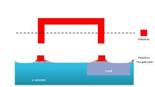
- CMOS technology uses both NMOS and PMOS transistors fabricated on the same silicon chip. The PMOS transistor is connected between the power supply and the output, and the NMOS transistor is connected between the output and ground. The NMOS and PMOS transistor gates are connected, forming the input of the inverter.
In the CMOS inverter and other CMOS logic functions, the output is connected through one or more transistors to either the power supply or ground. There is never a path from the power supply to ground (a short-circuit path). Furthermore, there is no current flow in the steady state, as the logic gate inputs are implemented as transistor gates, which are insulated from the source and drain terminals of the transistor.
Current flows only during switching from one state to another. Therefore, energy consumption depends on how often switching occurs and whether the logic switches in on each clock edge. Current flows only to charge or discharge parasitic capacitance in the circuit.
The logic gate output must always be pulled high to the supply voltage or pulled low to ground, and never allowed to float. A floating output results in an unknown intermediate voltage a the inputs of the gates downstream. This can cause both the PMOS and NMOS of transistors to be partially turned on, providing a short-circuit path from power to ground. To prevent this, the gate output must be connected through one or more transistors to either the power supply or ground.
Transistors are built using N-type and P-type silicon. In N-type silicon, a small fraction of the silicon atoms are replaced by an impurity such as phosphorus that has one more electron in its outer shell than silicon. A phosphorus atom easily gives up its extra electron, creating a negatively charged mobile carrier (electron) and an immobile ionized atom (phosphorus). N-type silicon can conduct electricity by means of its mobile electrons.
In P-type silicon, a small fraction of the silicon atoms are replaced by an impurity such as boron that has one fewer electron in its outer shell than silicon. A boron atom easily accepts an extra electron from a neighboring silicon atom, resulting in an immobile ionized atom (boron) and a positively charged silicon atom with an electron shortage. The missing electron is called a hole. A hole works just like a positively charged mobile particle because an electron from a neighboring silicon atom can jump into the hole, creating a new hole. P-type silicon can conduct electricity by means of its mobile holes.
Next video: CMOS Inverter Model Using Light Switches
• CMOS Inverter Model Us...
For more information, see the free textbook "Modern Semiconductor Devices for Integrated Circuits" by Chenming Hu: www.chu.berkeley.edu/modern-s...
Silicon & diamond unit cell atomic model, wafer/crystal orientation, Miller indices (100) (111)
• Silicon & diamond unit...  Наука
Наука


The 3D layout was really helpful for visualising how the CMOS inverter might actually look in real life. Great work.
This is the clearest video on CMOS Tech on RUclips! No wonder it has zero dislikes. Thank you sir! For clearing my concepts in 7 minutes what I couldn't do in 7 months XD
It is indeed very clear
For sure
Thank you very much for these visuals. Until now I was just mugging up things for CMOS but now i clearly understand what is actually happening inside. Great work!
i have almost seen 10 to 11 videos in youtube about the 3d modelling of CMOS, but this video cleared all the doubts..thank u sir...😊😊
Excellent work and explanation. These devices should always be explained with 3D drawings.
This tutorial is very easy to understand. Really helpful, thanks for sharing!
Ok thank you, i never understood why the PMOS gets conductive when you apply 0V at its gate, allways thought you need a negative voltage, but thanks to your video, you only need a negative potential difference between source and gate. (source is connected to bulk).
Thank you for the wonderful explanation .Great animated visuals👍
Awesome, great explanation. Thank you so much!!
Amazing explanation. THANK YOU!!!!
Many thanks for detailed explanation. Only after your video it was clear how Input and Output for logic gates works. Even after several times reading Harris and Harris book, it was really challenging to understand the current flow.
Yes, the Harris & Harris book works well as a reference -- it has all the information you need in compact form. The video is more like a college lecture, giving you time to digest the basic principles. In a good college course, the lecture and textbook are complementary.
Amazing amazing animation and explanation. Thanks a lot.
This is gold, thank you, sir
Governments spend millions on universities, just for a guy on youtube to beat the shit out of them ..
Great video, ty!
Great job! Thank you!
Very practical and useful
Great content, congratulations!
Really helpful and clear
THIS IS A GREAT VIDEO!!!
What a beautiful and genial explanation! 1000x thx :)
The bestt video...❤️
Extremely good video. Finally understood some things about this confusing goddamn subject, lol.
This video rocks !!
Sir you save my life
Mega cool, greetings aus Germany
Thank you 😆👍
Very nice
Super nice video! I was wondering what's in between the substrate and the metal connections? It looks like there is some gap in between but this has to be filled with something in a IC, right? Thanks a lot!
A hole is cut through the oxide and the metal connects directly to the silicon. In some cases extra dopant is implanted/diffused into the silicon where the metal makes contact.
@@graychang99 thank you! So basically SiO2 is isolating all the connections
Yes. To keep the diagram simple, I didn't show the SiO2 on which the metal connections are resting.
@@graychang99 it was a great video! By far the best one I've seen
Isn't it also very important to distinguish between depletion and enhancement type MOSFETs here?
Otherwise very good explanation! Thanks
Thanks for this great Video, I have one question! I have a computer science background and still struggle with basic concepts like current. In 5:20 (Input=1V) you say "A conducting path connects 0 Volts to the output. I have a hard time imagine, what does 0 Voltage mean? Does it mean no current is flowing at all? Or just a small amount? I think i have a problem with the concept of a Supply of 0 Voltage (nmos) which creates a conductiv path to the output. If basically nothing gets "pushed" (electrons) how can there be a flow of current?
See if this video helps: ruclips.net/video/Lvp_a_JkD2o/видео.html
How can I get these pictures, I need to make a presentation on CMOS, thank you
Freeze the video and use any screen capture program. Please give credit to the source in your presentation.
Where resistors and capacitors are connected in this?
Resistors and capacitors are not involved in CMOS inverter operation; there is no need for them. However, there is parasitic (unwanted) resistance in the semiconductor materials and parasitic capacitance in the P-N junctions that slow down switching between the 0 and 1 states.
negatively charged acceptor and positively charged donor ? donors are n-type impuriry and negatively charged
A donor atom donates a negatively charged mobile electron to the conduction band. The fixed-in-place donor atom becomes positively charged when it loses an electron.
I don't know anything
The DESCRIPTION section provides a little background on N-type and P-type silicon. For more background information, you'll need to consult Wikipedia or your textbook.