This is the BEST promotion vedio I've ever seen!! The warm, beautiful piano music flow with the cold, high tech machine really makes me chill. Great job!! Well done!!
When you look at the edge of what humanity has reached, you can only appreciate how lucky you are to be looking at one of the most amazing results of millions of years of evolution, including billions of attempts to answer questions that driven by our human curiosity "why and how"
And in reality all condensed in 6,000 years. If we can create this equipment, how infinite much More Is our Creator that created us!! Ask ASML what the odds are that this equipment would originate from a random big bang
@JanMol-rb4yo "Express that probability in one out of what number", you ask me? Okay, it's my opinion. I believe in science and everything that nature does, or doesn't do. So for me the probability that everything once started from a big bang and in which we are now, is one out of one. So, I'm 100% sure. And of course I respect your opinion. 😊👍🏼
.... and at Zeiss SMT, Trumpf (I think) and all the other manufacturers around the world producing crucial parts for theses machines. The laser tin-plasma part for example is from a US based company (if I recall correctly).
@@lawrencefrost9063 try building an EUV machine, when whole society told you to learn the word of God all day. Try building an EUV machine, when you have to carry water and grow food all day. Try building an EUV machine when the boss thinks it is a shitty expensive idea when success isn't obvious. Innovation happens in context of a society that enables it, then individuals take on the opportunity to act on it.
@@lawrencefrost9063 Right, for me, I'm proud to have a sucessor like ASML in my country and a F1 coureur Max Verstappen. Better than tulips, windmills and wooden shoes.
...did you really just write the awkward "humankind" word? Your ugly leftism is so sad. You do realize that "man" is contained right in the center of the word "huMANkind", right? Maybe you want to say "huPERSONkind"? Is that your style? Or just grow up and use the generic "mankind" since it means all people. You are simply such a sissy leftist that you can't even think. ps the word "personkind" actually means man as the root "son" is... oh, just look it up.
The movement of wafers and stepper is basically real time, it is not speed up. 185 wph. That is 26 seconds per wafer, and half of that time is just loading wafer, and metrology. The exposure is probably just 15 seconds per wafer. That is insane, if one considers that each wafer has hundredths of exposures. So stepper stage translates and aligns each exposure in like 200ms, to the nanometer. Insane. No idea how they do it, but a lot of smart hardware and software. And then you have all the other things, going on, hard vacuum, temperature control, light source and optics beyond precise, and all the other stuff. Crazy. And then you have things outside of machine that are also high tech like photosensitive resins, fabrication of the masks, etc.
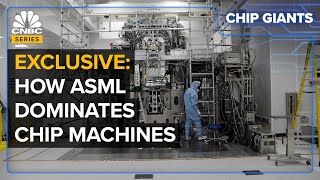
3 key components of an EUV machine is: the light source from Cymer, optic lens from Zeiss, stepper stage from Philips. The most technological advanced is still the light source and the complexity is just out of this world. This is somehow imo just alien technology 😂
In my humble opinion the greatest feat of technology ever is the transistor. I am greatftul for the genius people behind all this. Unbelievably astonishing job!
Absolutely stunning video. Truly a piece of art. As a Photonic Engineering student, I regularly come back to this video to get some motivation for studying!
It's amazing, thanks ASML for such a complex engineering marvel. It's jaw dropping. How does it feel to make such a complex machine with such precision and which is so important for mankind? ❤ASML
@@aero1000 There are a lot of more advanced technologies or machines in the world. The industrialization and practical scale of the ASML machines in combination with the cutting edge technology is what makes it this unique.
@@bobniks8411 I worked on both. ASML's EUV system is easily more advanced. Other than the sensing equipment CERNs hadron collider is a very very large infrastructure project which comes with its own challenges.
Tus machine has the best of all knowledge of humankind, applied physiscs (optics) chemistry, computer science, mechatronics, materials science, software. State of the technique.
Look at those wafer stages. Seems there have been some significant improvements there. Acceleration of 32G is very impressive. Transistor density and overlay improvements also notable.
The reticle stage is 32G. The wafer stage is 8g. Still incredibly impressive, but a factor of 4 lower accelerations, as you have a factor of 4 reduction in the image. Reticle stage is also significantly lighter.
Man...PPL just don't know It's the Pinnacle of technology..... masterpiece that is propelling our world....Without this we would have been living just like in 1930's.😢❤❤❤❤
Sub nanometer overlay is the surface of the layers on top of each other in 3D configurations. The transistors are of a size 8 nm even though now the measurement will be the density in mm3.
Super mooie video hopelijk kan ik vrijdag avond op de opendag komen ik had me aangemeld terwijl het vol was. Ik had geen plek ingevuld. Ben benieuwd of ik kan komen. Amazing video
according to reliable estimates the competition is at least 10 years behind. That means that the industry depends on ASML for at least 10 years… this is crazy remains from this machine.
1. EUV photomasks work by reflecting light... not like conventional photomasks which work by blocking light. 2. Photomask is covered with photoresist. Next it is exposed to laser light - maskless lithography with an electron beam. Exposed photoresist is removed and the unprotected areas are etched. The remaining photoresist is removed. Masks are inspected and later repaired using an electron beam... That process is basically shown in the video.
@@Verbatino Thanks for the reply. I'm familiar with how UV/DUV resists work. I think you missed my point though. At 1:28 it shows the images immediately appearing on silicon (or whatever it is) after write, which would normally not happen in lower energy systems until later development. I'm asking whether or not this is really how EUV resists work. Thanks!
@@iopredmanWell I see the pattern without developing in UV litho. If the printed pattern size is super small, it shouldn't be visible. However they may also print bigger structures by EUV. I think in the video it is due to illustration, like the purple EUV beam of 13,5 nm.
@@iopredman Well, if you get things right... then yes. Basically it might look as a simpler process on video... if you don't consider wild complexity of those EUV photomasks... and EUV optics... in vacum...
How many chips has inside the HIGH NA EUV machine? This machine has my algorithm too, being able to work so fast and with accuracy only the mathematical perfection can do that.
I wonder what kind of actuators do they use to get this accuracy&precision at this speed? Both wafer carrier-positioners and 32g acceleration of the reticle stage; seems like magic. But it is actually not magic, just state-of-the-art engineering.


Very glad to see the video finally public. It's been an honor working on it for the last couple of months.
This is the BEST promotion vedio I've ever seen!! The warm, beautiful piano music flow with the cold, high tech machine really makes me chill. Great job!! Well done!!
Bro i have applied for system performance Engineer job could you please help me with it
Impressive work. 👍
@@7INDERMusic I'm pretty sure they don't want anyone who starts a sentence with "Bro". 🤣
@@RetroJack cool😂
Finally a high quality PR clip about EUV NA application! Just in time for the shares boost (gained 50+ euros today)
Im just a dumb ass kid, but already made >9k with NVIDIA in the last 5 years.
How's your 50+ euros now?
When you look at the edge of what humanity has reached, you can only appreciate how lucky you are to be looking at one of the most amazing results of millions of years of evolution, including billions of attempts to answer questions that driven by our human curiosity "why and how"
And in reality all condensed in 6,000 years.
If we can create this equipment, how infinite much More Is our Creator that created us!!
Ask ASML what the odds are that this equipment would originate from a random big bang
?? 🤔✨
Everything emerged
from the Big Bang 💥
@@marcokrijgsman8099 could you please express that probability in a one out of a what number?
Oh god what is happening here
@JanMol-rb4yo
"Express that probability in one out of what number", you ask me?
Okay, it's my opinion. I believe in science and everything that nature does, or doesn't do. So for me the probability that everything once started from a big bang and in which we are now, is one out of one.
So, I'm 100% sure.
And of course I respect your opinion. 😊👍🏼
What a time to be alive. There are some serious geniuses at ASML.
.... and at Zeiss SMT, Trumpf (I think) and all the other manufacturers around the world producing crucial parts for theses machines.
The laser tin-plasma part for example is from a US based company (if I recall correctly).
@@L1m3r the light source is from Cymer (US)
Thank you ASML for this engineering marvel 🎉🔥🔥🔥 KEEP PUSHING THE LIMITS💪🏻
You're welcome
If that would have been a science fiction trailer, I would have believed it too. Amazing work ASML! Proud to be European.
Pride is for what you do not what you are. What are you proud of that you have done?
@@lawrencefrost9063 try building an EUV machine, when whole society told you to learn the word of God all day. Try building an EUV machine, when you have to carry water and grow food all day. Try building an EUV machine when the boss thinks it is a shitty expensive idea when success isn't obvious. Innovation happens in context of a society that enables it, then individuals take on the opportunity to act on it.
@@lawrencefrost9063 Looks like they pwned you - I'd say they should be pretty proud of themselves for that, but it doesn't seem to be a very high bar.
@@lawrencefrost9063 Right, for me, I'm proud to have a sucessor like ASML in my country and a F1 coureur Max Verstappen. Better than tulips, windmills and wooden shoes.
Then you should be ashamed too for colonisation, holocaust and 2 bloody world wars too as a European. Are you ?
Lithography is the most complicated bit of science the humankind has ever embarked on. What a time to be alive.
...did you really just write the awkward "humankind" word? Your ugly leftism is so sad. You do realize that "man" is contained right in the center of the word "huMANkind", right? Maybe you want to say "huPERSONkind"? Is that your style? Or just grow up and use the generic "mankind" since it means all people. You are simply such a sissy leftist that you can't even think. ps the word "personkind" actually means man as the root "son" is... oh, just look it up.
Where are all of my fellow Asianometry viewers at?
You bet we're here
Asianometry semiconductor geeks salute!!
Yes sir!
Right here with you, feeling amazed!
here!
Quality of the video is so crisp Bravo ASML pioneering in humanities best invention
The movement of wafers and stepper is basically real time, it is not speed up. 185 wph. That is 26 seconds per wafer, and half of that time is just loading wafer, and metrology. The exposure is probably just 15 seconds per wafer. That is insane, if one considers that each wafer has hundredths of exposures. So stepper stage translates and aligns each exposure in like 200ms, to the nanometer. Insane. No idea how they do it, but a lot of smart hardware and software. And then you have all the other things, going on, hard vacuum, temperature control, light source and optics beyond precise, and all the other stuff. Crazy. And then you have things outside of machine that are also high tech like photosensitive resins, fabrication of the masks, etc.
3 key components of an EUV machine is: the light source from Cymer, optic lens from Zeiss, stepper stage from Philips. The most technological advanced is still the light source and the complexity is just out of this world. This is somehow imo just alien technology 😂
THE BEST EUV MACHINE IN WORLD STRONG GREAT AMAZING ASML
There's is no other known company capable of doing EUV, certainly no High-NA.
Quantum is coming.
@@Weathering123next IS HYPER NA whit 0.75 NA.
@@Weathering123 quantum has been tried but it is not reliable
This is literal technomancy! Levering arcane knowledge in order to engrave runes that boost our capabilities. Truly awesome
Haha awesome way to look at it. I love that.
This is literally it 😂
This Video is a piece of Art.
I've watched many videos on how these machines work and I am completely blown away. It's engineering at a level that is almost magical.
In my humble opinion the greatest feat of technology ever is the transistor. I am greatftul for the genius people behind all this. Unbelievably astonishing job!
Absolutely stunning video. Truly a piece of art.
As a Photonic Engineering student, I regularly come back to this video to get some motivation for studying!
This is one of the most important videos on RUclips!
It's amazing, thanks ASML for such a complex engineering marvel. It's jaw dropping.
How does it feel to make such a complex machine with such precision and which is so important for mankind?
❤ASML
Seriously great work by all the wizards at ASML, congrats guys!
The work the team does at ASML is unparalleled anywhere on the planet!
Impressive work ASML! Proud you of team❤
One of the most technologically advanced and complex machines on the planet, for sure!
*The. Name me a technology/machine more advanced.
@@aero1000 There are a lot of more advanced technologies or machines in the world. The industrialization and practical scale of the ASML machines in combination with the cutting edge technology is what makes it this unique.
@@cornee111120 Give me some examples then? I'm waiting.
@@aero1000 Probably CERN's large hadron collider might be of the same caliber as ASML's machines.
@@bobniks8411 I worked on both. ASML's EUV system is easily more advanced. Other than the sensing equipment CERNs hadron collider is a very very large infrastructure project which comes with its own challenges.
This is fantastic and marvelous. Great tech lies in the future
Tus machine has the best of all knowledge of humankind, applied physiscs (optics) chemistry, computer science, mechatronics, materials science, software. State of the technique.
This is absolutely mind-blowing. Human ingenuity at its finest.
Absolute pinnacle of engineering
This gives me goosebumps every time I watch it.
the movement on that reticle stage is amazing!
정말 정말 대단합니다.
회사와 사원들에게 평범한 시민 한사람으로 감사드립니다.
Look at those wafer stages. Seems there have been some significant improvements there.
Acceleration of 32G is very impressive. Transistor density and overlay improvements also notable.
Is moving extremely fast with nm accuracy.
The reticle stage is 32G. The wafer stage is 8g. Still incredibly impressive, but a factor of 4 lower accelerations, as you have a factor of 4 reduction in the image. Reticle stage is also significantly lighter.
Pure inspiration.. very beautiful technology ❤
That video is astonishing, pleasant to watch. Good job
ASML pioneering AI technology, beautiful video 👏
I own ASML stock. I will keep buying it without doubt. ASML is the future.
Until China attacks Taiwan and seizes assets.
Ponzi assets
No evidence. There is always a mother who gave birth to an inferior human.
Impressive. Very impressive.
Glad to see more public related communication
wow .. that anamorphic optics and Hi-NA EUV is wow
Amazing technology ❤
I love it, GO ASML !
Whoever came up with the idea of blasting droplets of molten tin with a laser to produce EUV light deserves a Nobel Prize😮
Nicest KT i've seen in a while
Absolutely fascinating!
The most beautiful thing in the universe
is not science is Art!! Congratulations!
Man...PPL just don't know It's the Pinnacle of technology..... masterpiece that is propelling our world....Without this we would have been living just like in 1930's.😢❤❤❤❤
Yeah, you said well, can't wait for hyper na 0.75 NA in 2030.
Proud to be part of ASML for atleast a year now. Its been a wonderful journey!
Keep it up buddy, you are part of the GOAT company.
How Fantastic!!! Great Job ASML & Friends!!!
I made a few of the major components of this machine. I can actually see them in this video, pretty awesome.
This is Soo Unbelievable!!! So Awesome!!
it's really amazing to see the process😮
I love ASML so much
What an incredible achievement! Congratulation!
Simply amazing!
so beautiful!
Insane technology
This is soo amazing
Why arent the wafers squared?
Is this a completely new machine, or an upgrade package to existing machines?
New
stunning machine
We live in the future!
As close to magic as humans have ever gotten.
Sub nanometer overlay is the surface of the layers on top of each other in 3D configurations. The transistors are of a size 8 nm even though now the measurement will be the density in mm3.
🎉congratulations
This is art.
THIS is the Great Wonder of our times!
Super mooie video hopelijk kan ik vrijdag avond op de opendag komen ik had me aangemeld terwijl het vol was. Ik had geen plek ingevuld. Ben benieuwd of ik kan komen. Amazing video
Can someone tell me if there is there a more complexe machine on earth?
Maybe the greatest technology humanity has ever made
素晴らしい
ASML 진심으로 갈거다
You did Not Show the Optics and How they work 😊 - Greetings from a small town in south Germany - nice Animation btw 😮
It's secret ;-)
How much does it cost and where do I buy one
Can I buy this machine through a reseller or directly? Time to bake my own chips.
It's only 380million usd. Certainly a bargain, if you happen to be Chinese
@@Hippida I started to read 150, then 200 now 380 million dollars.
Wish I could work on ASML machines but you guys rejected my application w/o an interview 😢
keep trying
maybe they thought you were a Chinese spy 😊
what a piece of engineering marvel. almost alien-like.
Engineering Marvel and Pinnacle of human intellect
This was so beautiful....
Epitome of human engineering😮😮
bone of humankind ❤
Yes we can :)
according to reliable estimates the competition is at least 10 years behind. That means that the industry depends on ASML for at least 10 years… this is crazy
remains from this machine.
How does 8nm resolution allow for 2nm chips?
2nm is marketing, 8nm is real.
Awesome!
Beautiful !🤯
Does EUV resist actually immediately create an image like this without development or is that just an artistic representation?
I had the same thought.😄
1. EUV photomasks work by reflecting light... not like conventional photomasks which work by blocking light.
2. Photomask is covered with photoresist. Next it is exposed to laser light - maskless lithography with an electron beam. Exposed photoresist is removed and the unprotected areas are etched. The remaining photoresist is removed. Masks are inspected and later repaired using an electron beam...
That process is basically shown in the video.
@@Verbatino Thanks for the reply. I'm familiar with how UV/DUV resists work. I think you missed my point though. At 1:28 it shows the images immediately appearing on silicon (or whatever it is) after write, which would normally not happen in lower energy systems until later development. I'm asking whether or not this is really how EUV resists work. Thanks!
@@iopredmanWell I see the pattern without developing in UV litho. If the printed pattern size is super small, it shouldn't be visible. However they may also print bigger structures by EUV. I think in the video it is due to illustration, like the purple EUV beam of 13,5 nm.
@@iopredman Well, if you get things right... then yes.
Basically it might look as a simpler process on video... if you don't consider wild complexity of those EUV photomasks... and EUV optics... in vacum...
What is this song called?
I wonder what the next material will be (the source of the UV emission).
Wat is het thermodynamische effect op reflecterende oppervlakken?
30%, dus een hele sterke source nodig 🔦
Wow, will this enable 0 nm process nodes ?
0,5nm, after that you need HYPER NA 0.75NA 2030+years.
In a thousand years, people will wonder how did we get this alien technology?!
I can see the end of Moore's law, which was more of an optimistic forecast than anything else
How many chips has inside the HIGH NA EUV machine?
This machine has my algorithm too, being able to work so fast and with accuracy only the mathematical perfection can do that.
I wonder what kind of actuators do they use to get this accuracy&precision at this speed? Both wafer carrier-positioners and 32g acceleration of the reticle stage; seems like magic. But it is actually not magic, just state-of-the-art engineering.
かっちょいい~!!
I wish this clip was one hour long.
Great CGI!
Onwards to 3nm and Beyond
Now the measurement is changed because of 3D chip designs and all is done with number of transistors per mm3 or cm3.
Literally putting lightning inside rocks to make them think
am confused where is the mask applying and cleaning? or it doesn't need that?
I'd like a free sample machine but only if delivery is free.