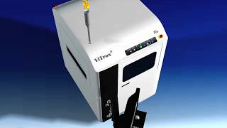
eSL10™ E-beam Wafer Defect Inspection System
HTML-код
- Опубликовано: 28 окт 2020
- Today’s leading-edge ICs are fabricated using intricate shapes and new materials, with structures that are smaller, narrower, taller and deeper. This complexity demands innovative defect inspection solutions. The eSL10™ e-beam patterned wafer defect inspection system captures and identifies defects not found by other inspectors, reducing the cycle time required for solving critical yield or reliability issues. By providing a deep understanding of critical defects early in the chip manufacturing process, the eSL10 helps accelerate time-to-market for innovative electronic devices. Learn more at www.kla-tencor....
Watch the latest videos on KLA.com and explore our channels in the KLA Media Room: www.kla.com/me...


