Это видео недоступно.
Сожалеем об этом.
PCB High-Speed Design Basics | PCB Knowledge

HTML-код
- Опубликовано: 5 авг 2024
- Have you ever noticed that when we introduce some PCB designs or techniques like back drilling or teardrops, we often see a sentence like “it can be applied to high-speed applications”? But how much do you know about high-speed PCB design?
This video will introduce some basic information about high-speed PCB design, so let's get started.
Chapters
00:00 Intro
(Considerations in high-speed design)
00:46 Signal Integrity
01:39 PCB Substrate
02:38 Placement of large ICs
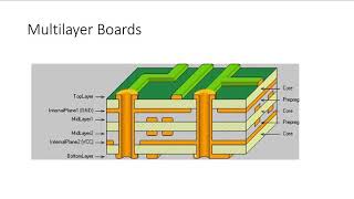
03:35 Stack-up
Website:
www.pcbway.com
www.pcbway.es
www.pcbway.ru
www.pcbway.fr
www.pcbway.jp
Subscribe and follow us to keep updated with the latest news and promotion:
Facebook: / pcbway
Twitter: / pcbwayofficial
Instagram: / pcbway
VK: pcbway
TikTok: / pcbway


What are your considerations when designing high-speed PCBs? Any tips and tricks are welcome to be shared below.
I think for the 5-layer stackup, it is better to have a ground between each two signal plans.
when will HS design will be as easy as web development ?!
but you master web development. that's also a cool thing!
It's an unfinished video😅
Thanks for the feedback. Is there anything we can improve for this video?
🙏👌