Mastering KiCad: Design & Build Your Custom Stereo Amplifier Board!

HTML-код
- Опубликовано: 12 июл 2024
- I've been working on a custom stereo I2S amplifier board using the MAX98357 IC. I've had the first version manufactured by www.PCBWay.com/?from=atomic and now I need to design version 2 - I'll get this manufactured by PCBWay again.
PCBWay provide sponsorship for the channel that helps pay for components and software.
There's a couple of things I need to fix from my first design. I made the boards far too small (got carried away in the PCB layout stage and thought I was being clever). So I'm going to fix that in this version.
I always want to learn to use KiCad, so this feels like a good opportunity to do that.
0:00 Intro - what are we trying to do?
0:38 Why KiCad - what's so special about KiCad?
1:10 Geting KiCad setup for PCBWay
1:46 Adding a new symbol to KiCad for the MAX98357
2:38 Designing the schematic for our board
4:33 Assigning footprints to the symbols
5:18 Converting the schematic to a PCB
5:34 Using a DXF file to make a custom board outline
6:08 Laying out the PCB
6:52 Ground planes/Copper pours
7:13 3D Viewer and adding missing 3D models
7:41 3D Export for Fusion 360
8:07 Adding the mounting holes
8:48 Labelling the pins
9:03 Gerber Export
9:50 Creating the BOM file
10:40 Component positions
10:57 Order submission to PCBWay for manufacture and SMT assembly
11:20 Final costs and sanity check
11:43 What do I think of KiCad? Would I use it again?
----
Patreon: / atomic14
ko-fi: ko-fi.com/atomic14  Наука
Наука


DId anyone say that this is one of the best best KiCad intros. It covers everything a beginner like me would need. Thanks a lot.
Been using KiCad for 6/7 years now. It's my favourite PCB design tool!
I did really enjoy using it. Will use it for my next project - might try version 6.
Short and sweet 😃 Having designed 20 or so boards in Eagle, I had to modify a KiCad board , and then designed a couple of boards from scratch I’m beginning to like it now. I originally followed a 30 min tutorial , took me about 3 hours to design the board and add a few of my own things to it . The second board was somewhat easier , and simpler. I’ve picked up a few extra points from your video , so Many Thanks
Great, I'm glad you found it useful. I find with all these things, there's an initial hump to get over where lots of things are just different enough to be frustrating, but then after a few tries it becomes second nature and starts to flow properly. My problem is often having the willpower to get over that initial hump...
Extremely informative, many thanks. I keep toying with moving from EasyEDA to KiCAD for the same reasons as you did, but each time I've had a quick look, I've always gone back to EasyEDA. After watching your video, I'm inspired to give it another go.
Definitely wasn't as bad as I was expecting :) I'm going to give KiCad v6 a go - it's not released yet, but from the sounds of things it a good step forward.
Of course you have. EasyEDA has a powerful built-in library of parts.
I'm in the same boat. Adding parts is such a hassle in KiCad compared to EasyEDA. A few things annoyed me in EasyEDA as well (like the bottom layer view) so that I gave KiCad 6 a try, but now the new EasyEDA Pro is available, which solves a lot of the EasyEDA issues, so I went back to that one. I'm so much quicker with it.
More PCB design videos: ruclips.net/p/PL5vDt5AALlRdT8FjdJQahfIuOuSswRdbL
Interested in ESP32 Audio: ruclips.net/p/PL5vDt5AALlRfGVUv2x7riDMIOX34udtKD
Looking for all my ESP32 projects: ruclips.net/p/PL5vDt5AALlRdN2KyL30l8j7kLCxhDUrNw
You can see version 1 of the board here: ruclips.net/video/2ZdfMJNfCWg/видео.html
Thanks for making this video. I've decided to make the leap from my crusty old Eagle CAD, so you showing the setup for PCBWay (which I also use) was extra helpful. I found your channel because you commented on one of my videos, and now you're helping me out with one of your videos! Go go gadget Maker Community! Woot. I think your accent makes for great voice over.
Things to note:
1. You can create the identifiers using the annotate schematic option.
2. I'm pretty sure you do not need to generate a netlist in kicad. I remember reading that kicad does this automatically since version 4.
3. Something you might want to look into is the "edit symbol fields" feature in eschema. It's great for aiding in BOM generation as you can insert custom fields for later. It can save a lot of effort compared to doing it in excel.
Just my tips after using kicad for a few years.
Thanks Jonathon - great tips! Exactly what I was hoping for from the video.
When adding pins to the connector, create first one and use the INSERT key to create each of the others needed. KiCad 6 has many improvements and, shall I say, differences. No more Netlist button - File/Export/Netlist.. now. Better to change sooner than later before you get attached to KiCad 5 ways of doing things. Great video. I just subscribed and will be looking around for other gems.
Wow the video is really good! And u seem to know a lot about audio (and you even have ESP32 I2S videos that I was actually looking for). New sub
Thanks - I've got some more audio videos in the pipeline.
I use KitKat when it won't draw a new line I just bite a bit off and carry on ;-)
It's Keycad, the guy who started the project named it after a family friend who died, gentleman's name was Ki and its pronounced ' KEY ' but I guess it dosent matter! this was a great tutorial and I will disable the "generous" courtyards as well, something I have never found but now I know it's there !....cheers.
Thanks! And thank you for the background history. There's always an interesting bit of history behind the names of things. The courtyard setting is an interesting one. There are definitely good reasons to have space around connectors, but it's annoying it's a DRC error rather than more of a warning.
@@atomic14 Oh yes its useful, but as you say I would prefer Kicad to point it out, as opposed to an error.
I liked your comments between sections of the video, they are very amusing 😄
@@RaDoNkron Best bits of the video ;)
For the symbol IDs (question marks), you can use the Tools - Annotate option to set them for you.
Also there are two types of labels available in KiCad, global (what you used) and sheet specific. This is mostly applicable in complex designs with multiple sheets.
That's handy to know, I need to dig a bit more into the annotation side of things as I think that will make my BOM file generation a bit slicker as well. I had a vague idea about the global and sheet specific labels but wasn't quite sure how to use them. One thing I did miss was being able to draw boxes around logical groups of components. I don't think that's currently possible and your supposed to use multiple sheets instead to organise things?
@@atomic14 In the tool palette is a blue dashed line box icon which you can use to draw boxes/lines/etc, hotkey for this tool is | (pipe).
Multiple sheets (or hierarchical sheets) is great for complex projects and can help organize the schematic into sections (power, inputs, outputs, etc) in a similar manner to how you used boxes in the other EDA tool.
Perfect - the dotted line was exactly what I was looking for.
Big like for this one, thanks a lot!
Thanks! Much appreciated
I made it with Eagle PCB. A good program and for a long time you could use it for private use, small board size and only 2 layers for free. The purchase version is too expensive for infrequent use. Then I tried easyEDA.
A cramp with a trakpad. Good if I want to throw one IC, two capacitors and three headers together ... But Eagle is much better. But my Eagle version is just a trail and restricted.
But I think I'll give KiCAD a try.
As a guy just starting, this was a bit ‘fast’ for me, and took in some operations I cant see myself using, having said that, its always good to know about something..
thank you! i loved this video
Vote up, nice video clip, thanks for sharing :)
Yeah but I do like easyeda's really good connection with LCSC and JLCPCB, if KiCad has also really good connection and a better ui now maybe I'll give it a go, but I dont need to since i probably wont make many pcbs
Such a good video!
great video! thanks!
Drawing the outline with rounded edges is easy with the draw arc tool if you have selected a proper edit grid size.
Interesting - I'll give that a go.
Well done!
Thanks :)
The BOM entry for mounting holes is for if you have something like surface mount standoffs.
What kind of fastener are you using for mounting? It doesn't look like there's room for a screw head.
You may consider trying EagleCAD built in Fusion 360. You can do the same without exporting 3d view, just insert it in your enclosure
nice job pal
'KeyCad' is CAD program by Softkey for Dos and windows so it is possibly pronounced the other way. I actually found a boxed copy of KeyCad (not KiCad) at a car boot sale a couple of years ago.
First time KiCAD in a video - Gutsy move ;)
I had a couple of cheeky test runs first :)
Generation of the net list is a deprecated step in recent versions. If the schematic is saved you can open PCB New and just hit the Update button.
And I think you can edit the symbol and include part numbers, so BOM generation already has the values. Bonus, if you update the symbol which is in the library, you get the values every time you use that symbol.
That's very handy - I should have had a look at the symbol editing as well, that sounds like a very sensible way to go.
If i‘d to start with KiCad today, i‘d probably jump directly onto version 6 (nightly build) - release expected ‚really soon now‘… :-)
Looks like I'll need to do another video soon!
@@atomic14 It'd be interesting to see if any of the, niggles you came across when designing the PCB have been fixed in v6.
Seems like EasyEDA is much more user friendly.
I also started on EasyEDA and then switched to KiCad for later projects, and now that I'm used to KiCad I can't stand the way zooming works in EasyEDA. I also use the same trick to scroll and pinch to zoom with my trackpad, and it's so much more intuitive.
I'm not sure why it's not the default. I was trying another piece of software yesterday where to pan to have to hold down the space bar and then move the mouse - completely bonkers.
@@atomic14 I'm assuming it was written in a world of scroll wheels, not multi-touch trackpads.
Holy crap. Take a shot everytime he says "footprint". Said it like 50 times 4:34 it was at least every other word said lol
The possibility of exporting a STEP/STP file is something that draws me to KiCAD... I'm yet to start using it and the video is quite compelling 😅
EasyEDA exported OBJ files usually wreaks havoc on Fusion 360, since EasyEDA exports all files in "mills" even though we explicitly specify units as mm, while Fusion 360 does not support/read "mils". Also to add to the problem, the generated OBJ has least resolution and renders horribly when opened on Fusion (or any software like Meshmixer or even Windows 3D viewer/builder). Scaling never works well and sometimes with disastrously off measurements
Yes, it's pretty dreadful. The few times I've tried it have either made Fusion360 grind to a halt or resulted in terrible meshes. The output from KiCAD is really nice.
Thanks this will come in handy. BTW KiCad 6.0 is out :P
I just use lines and arcs to created a rounded PCB outline, pretty simple to me. Start off with a rectangle, put the right arc in each corner, then delete the rectangle and join up each arc with lines
KiCad 7 now has a "Fillet Rectangle" feature, and it's as awesome as it sounds.
You can easily do that curved corner outline. Just use lines and Arcs. Don't quite understand why you said it can't be done.
Using fusion 360 is not necessary, you can do the same outline within Kicad.
Sir, thanks for such a nice video.
As you do, I am also considering move to kicad from easyeda for 3D model export.
Another choice could be fusion360 electrical design.
I want to know if you ever tried it.
If yes, Which one do you prefer and what.s the reason?
I’ve only briefly tried the fusion360 electrical design. I did not find it very intuitive or easy to use - but I did not put very much effort into using it. I think most people are using KiCad so there’s a much larger community to get help from.
@@atomic14 Appreciate for your kind answer. Now I got to know what to choose!
Definitely going to replay this video with heavy use of the pause button as an EasyEDA to KiCad tutorial and see if I can make sense of it as you have., (I pronounce it [K-eye Kad] though I have no idea if I'm correct).
KeeCad is the correct pronunciation apparently. Good luck with the switchover!
@@atomic14 Thanks! And of course ... [Kee-Kad] makes perfect sense with the spelling of Ki-Cad vs. Key-Cad ... Though I'm sure there's a cultural ignorance gap in there somewhere on my part ... lol
I had no idea the board could be exported for Fusion. Just moved to KiCad, so extra happy. Had some weird things happen, which I need to figure out why. Like the grounds not connecting together on some switches. Other than that, I’m finding KiCad much better than EasyEDA
Nice
KiCad is very sophisticated but I find that simple things are not done well.
For instance :
-moving a symbol in schematic :
.before v6.0 the connections were lost
.v6.0 the connection loose orthogonality and became unreadable
- routing manualy a track in PCB : if you want to modify the route, the old route stay and you have to manualy delete every segment of the old route.
Perhaps I dont use it correctly ?
Do you know how to import the schematic from EasyEDA to KiCad?
I don't know if that's possible, there seem to be some scripts for converting footprints.
Have look for the small symbol C_small or R_small which is a nicer size.
Ah yes, that's much nicer!
I'm a novice. Seems to me EasyEda is quicker, less tinkering than KiCad. I can't find video comparing the two systems side by side. So I will just stick to my own experience with both. EasyEda is more workflow friendly including full access to LCSC component library with footprint and prices and ability to create the BOM without the need to tinker it as in this video.
It's 2023 outside the window, and the best thing for a beginner and beyond is to use EasyEDA. Because it is a free online tool - component databases are available to you immediately. You, in most cases, will not have to draw your own components. There is also a 3D render of the PCB with components. And you can immediately order the manufacture of the board and even assembly with components.
>>Main screen turn on>are belong to us
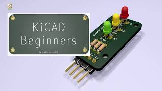
I think I got confused as the Adafruit board is quite short so the the ends of the headers are very close to the edge. And then I just went a bit mad and made it made it too thin :)
Also, glad you got the reference, wasn't sure how obscure it was :)
@@atomic14 While the reference isn't obscure, it does put those who 'get it' into a certain age-group ;)
Could show how make Esp32 board in kicad? Thanks
Definitely - was thinking that would be a really great video.
you can automatically annotate ? labels by clicking on the annotation tool next to the "bug" button
Perfect - that makes a lot more sense. I'm used to the numbers automatically incrementing as you add components.
The originator of KiCad pronounces it keecad. He's French.
Current project leader Wayne Stambaugh also says "key-cad". He's American.
I think you are correct - "key-cad" is the one.
@@Tim_Small The first sentence provided authority on the project. The second sentence removed authority on pronunciation !
@@frogandspanner You can see him talk on KiCad at it Fosdem in Brussels every year if that makes it better? Seriously though, I would recommend viewing those talks, they are on the Fosdem website and also RUclips.
KeeCad
👍
I found the autorouter from Easy EDA a step ahead.
I've not actually used the autorouter - I really should give it a go and see how well it performs.
@@atomic14 Easy EDA autorouter is fabolous, you can set track width, clearences (and it works very well), exclude nets from the autorouter, give some special config to some nets, ecc. ecc. You should give it a try. :)
Take off every ZIG!
👍
Hi Atomic, are you going to share the files of this version 2.0?
Definitely - I’ll upload them to OSHWA
@@atomic14 Great atomic. Regards
I've put the files on GitHub - raise an issue if it's not quite right, as I'm not sure what files need to be there - github.com/atomic14/stereo-i2s-amp-board
@@atomic14Thanks. Lately i was working with Easyeda to kicad, it was a bit difficult but it's better
@@atomic14 Idea: Put a link to this video in the readme.
KeeCad.
👍
@@atomic14 Great video btw.
Hi sir, how to add name of the pin sir?? Like pin 1 5v, pin 2 gnd and other sir. I want to make on manufacture ocb like a jlcpcb
I have done countless boards on the job and still end up with little green terminal blocks hanging over the edge.
PCB mistakes seems almost inevitable. I've now learnt to hold off submitting anything for manufacture until the following day. I invariably find some stupid mistake when I check the next morning.
@@atomic14 On the job we use an old LPKF prototyper still running Windows XP. And that's for on the spot non-production stuff. For the last three years I watched a PCB for a new product line go through several revisions because of problems that popped up and those designed had entire teams of engineers and even a CAD wizard who renders everything in 3D to check for clearances and there are still problems! I learned there is nothing a lone person using free stuff should be ashamed of.
since your in Fusion 360 any way, why not just use Fusion 360 electronics?
I started using kicad since using easyeda means too much dependency on Chinese applications
Well you still use their pcb manufacturing services
Not really. In my country India we do have many local pcb manufacturers upto 4 layers
@@sayantanmaiti2513 but it's not affordable
Кі-Кад 😁
key CAD, end of story !
import a netlist ? are you using KiCAD 4? Btw, look up their live streams. It's pronounced KeeCad
Its the KeeCad
👍
i say KuhCad
nah im kidding KeeCad :P
Prononce it as "Keecad" as it's a French name. :-)
The pronunciation of KiCad is sort of an in-joke within the KiCad community. Both K-eye-Cad and Key-Cad are valid pronounciations with two informal groups within the community professing allegiance to each of the pronunciations. Makes for a good mock argument to steer actual flame-wars towards to defuse situations.
When you did your project you created a netlist from the schematic and then loaded the netlist into the pcb. This is now a depreciated workflow. You can skip the whole generation of the netlist file and update the pcb from the schematic with a single menu item. You can't really update the schematic from the pcb if you wanted (for example) to swap pins on an IC. KiCad's native workflow has information flow from the schematic to pcb.
I love a good flamewar. Tabs vs Spaces is still a favourite.
Kitkat? KiCad?
I wish everyone would stop using Labels. Use wires or buses. I pronoun it as "Kee- Cad" Is open source it works, if you want better buy it.
It is free please don't forget that.
That's one of the reasons why I'm keen to use it. Free and open source - very deserving of support.
where is pcb design?
Way too fast. I had to keep pausing and rewinding.
Asians usually pronounce the letter i as a vowel "E", while Americans use the 'i' sound. IE we pronounce the name of the Japanese camera maker N-iEYE-CON, while the Japanese say N-knee-con. I think Europeans usually go with the Asian pronounciation. Same for those 'down under'.
I didn't like the symbol I found for the 74HC4053, so I tried to design my own. This is a 3 unit SPDT fet switch (3PDT?), with a separate control pin for each switch. So I tried to create a part with three 'units'. Each was drawn as a SPDT switch, with a dotted line for the control pin. Actually, I also needed to add common VCC, VSS, Ground, and Enable pins, which would be the 4th unit in the part. So I tried clicking on the 'non identical units' box so I could create the three switches and the power / enable pins. Somehow, the editor still tried to duplicate the first unit I created for the next three. Hopefully, I'll figure this out yet. I also had an issue getting the grid snap the same for my new symbol as for the schematic so I could get the wires to land right. UGH!
I just use the standard footprint for the package of the part. IE: all TSSOP-16 pin parts should use the same footprint, no need to duplicate it for each part. At least if you have the pin numbers correct for both the footprint and the part.
There's something about footprints, both the management and custom ones, that seems to be unfathomably complicated. It should be easy, but every time I do it I hit problems. I had big problems in EasyEDA trying to get a footprint for the ICS43434 - trying to make a circular pad seemed to involve way more clicks than it should.
For the amplifier IC I should have just associated it with the standard footprint for the package - I guess that's why we have standards after all!
/ˈkiːˌkæd/ or KEE-Kad - similar if it would be pie-cad then ki-cad :)