One concept at a time per video -- this is a good teaching technique which you seldom see elsewhere. I'm not a student, nor an expert, but I love these videos, which I just watch out of interest. Thank you Mahesh!
The first diodes were vacuum tubes. The cathode was heated up so that it "evaporated" elecrons, and the anode would collect electrons only if it was at a potential higher than the cathode. And there were vacuum tube triodes as well, which were used to amplify. I am old enough to remember taking vacuum tubes from a television to a store to test which one burned out.
Sir please clear my doubt. When forward biased, the depletion region voltage 0.7 is opposed by the applied voltage. But when the applied voltage is less than the cut off voltage, the current should be zero. Only when the applied voltage overcome the cut off voltage current should flow through the circuit. Until that no current should flow through the circuit. That is, when forward biased, the depletion layer becomes narrow.But it still exist.So some more electrons and holes enter the depletion layer and recombine. But eventually the current due to majority charge carriers should be balanced by the minority charge carriers moving in the opposite direction.So equilibrium should be reached once again and no net current should flow through the circuit.
Without any applied voltage, the two currents (drift and diffusion) cancel out, giving net current zero. So when you forward bias, however small the voltage be, the depletion region shortens, and diffusion increases. The equilibrium is now lost, and a net current flows. Also note, the recombination of the majority carriers IS responsible for the diffusion current. It's the recombination that maintains the concentration gradient required for diffusion current. [If this sounds confusing, there is a video on '' explaining it in great detail]. Happy to answer more questions.
Sir please clear my doubt, in our book it is written that as we increase the reverse bias current is going to be increased as minority carriers attain high velocity and knock down the bound electrons from covalent bonds and the current increases. How is this possible and is this even right?


The semiconductor series is really awesome Mr.Mahesh, you really deserve your current post of Khan academy India science lead!
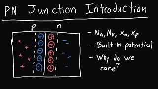
6:35 Diode comes from the greek word "δίοδος"
δι (two) is a prefix and οδός (ode) means road
Amazing video! We need more videos on Khan Academy India!
Beautifully explained in depth ❤❤..that too in a structured manner..has made the chapter crystal clear to me😊😊
One concept at a time per video -- this is a good teaching technique which you seldom see elsewhere. I'm not a student, nor an expert, but I love these videos, which I just watch out of interest. Thank you Mahesh!
Such an amazing video!!!
wow u have explained everything so nicely every graph every point of ncert
You are trully a bleesing for physics students.keep up the good work!
The first diodes were vacuum tubes. The cathode was heated up so that it "evaporated" elecrons, and the anode would collect electrons only if it was at a potential higher than the cathode. And there were vacuum tube triodes as well, which were used to amplify. I am old enough to remember taking vacuum tubes from a television to a store to test which one burned out.
Sir please clear my doubt.
When forward biased, the depletion region voltage 0.7 is opposed by the applied voltage. But when the applied voltage is less than the cut off voltage, the current should be zero. Only when the applied voltage overcome the cut off voltage current should flow through the circuit. Until that no current should flow through the circuit.
That is, when forward biased, the depletion layer becomes narrow.But it still exist.So some more electrons and holes enter the depletion layer and recombine. But eventually the current due to majority charge carriers should be balanced by the minority charge carriers moving in the opposite direction.So equilibrium should be reached once again and no net current should flow through the circuit.
Without any applied voltage, the two currents (drift and diffusion) cancel out, giving net current zero. So when you forward bias, however small the voltage be, the depletion region shortens, and diffusion increases. The equilibrium is now lost, and a net current flows.
Also note, the recombination of the majority carriers IS responsible for the diffusion current. It's the recombination that maintains the concentration gradient required for diffusion current. [If this sounds confusing, there is a video on '' explaining it in great detail]. Happy to answer more questions.
Finally understood this chapter after so long!
love you sir that's it.
Great explanation....thank u so much for such an explanation 🙏🙏🙏
Mind blowing lectures
Sir please clear my doubt, in our book it is written that as we increase the reverse bias current is going to be increased as minority carriers attain high velocity and knock down the bound electrons from covalent bonds and the current increases. How is this possible and is this even right?
It is actually path. It comes from the greek word Δίοδος which means 2 and road-path.
Great video thanks!
Di means 2 and ode means the two symbols represent (+) which is anode(ode) and (-) which is cathode(ode)
Thank you
Superb.....
Awesome
1:44 Sir ,is the cut in voltage at forward biasing is equal to the barrier potential of the semiconductor?
Ig so
name of the app?
sir plzzz can you make a video on a photo diode
dope
👍👍👍
🙏🙏🙏🙏
depletion layer don’t disappear. 1:24