LVS (Layout vs Schematic)Check in Cadence | using Calibre | PEX | Post Layout Simulation in Virtuoso

HTML-код
- Опубликовано: 8 апр 2018
- This tutorial shows how to do Layout vs Schematic (LVS) checks in Cadence Virtuoso using Calibre tool of MentorGraphics. Solving of DRC violations, Parasitic Extraction (PEX) in Cadence using Calibre and Post Layout Simulation has also been demonstrated in this video.
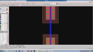
This is 6th session of this Layout series of Videos, In continuation with session-5, some DRC errors were introduced and shown how to remove those errors. Then Layout Vs Schematic (LVS) check has been done using Calibre. Now after the layout is DRC and LVS clean, we moved to Parasitic extraction (PEX) step using the Calibre tool. We extracted the parasitics associated with layout and visualized that. A post-layout simulation has been performed after the PEX and compared pre-layout and Post layout simulations output together.
Links of all the videos in this series are as follows
1. Layout of nmos:
• Layout design of nMOS ...
2. Layout of pMOS
• Layout Design of pMOS ...
3. Layout of BJT
• Layout design of BJT (...
4.Pcell Implementation
• Pcell (parametrized ce...
5. DRC check, Simulation and other explanations
• Design Rule Check | DR...
6. LVS, PEX and Post Layout Simulations
• LVS (Layout vs Schemat...
* Integration of Calibre tool in Cadence Virtuoso
• Calibre EDA tool | Ins...
If you feel this video is relevant to your domain and useful, please like the video and subscribe to the channel and share with your connections.
Your queries/suggestions are most welcome in the comment section. Please comment on your reaction.
====Connect with us==========================
All on one page: www.teamvlsi.com/p/contact_8....
Blog: www.teamvlsi.com
Facebook Page: / teamvlsi
WhatsApp Group: chat.whatsapp.com/C6etLHR6oAf...
Telegram Group: t.me/teamvlsi (Or search team VLSI on telegram)
Email: teamvlsi2014@gmail.com
==============================
#LVS #PEX #PostLayoutSimulations


Thank you! Need a video for LVS debugging, rather than running a layout that was already clean. Also, maybe more than an inverter. Great beginning.
Thanks Berry,
Sure, we will try to publish the same.
I am getting error that number of ports are not same. In layout it is showing 0 ports and in schematic 4 ports while both are having the same number of Pins.
Sir..my pre layout and post layout is mismatch. I tried inverter aslo.but pre layout & post layout mismatch. I am using SCL PDK. I don't know why it is coming like that
Hi Arul,
Kindly analyze the LVS report and try to understand the exact reason.
Sir..I am Arul working Project staff in NIT Delhi
All the best Arul. Good place to work and you are having ample opportunity to explore the VLSI stuff. Keep exploring... Keep learning.
@@TeamVLSI yes sir..Thanks sir..
@@TeamVLSI sir..I got.output sir..
Sir..I want ur help. Please reply me
Sure Arul.
Please ping me personally on WhatsApp.
@@TeamVLSI yes sir..
Sir audio level is very low.
please sir update this video.
I am not finding S1,S2,S3,S4 video in this channel.
Please sir check once.
If all videos are in serial, then beginners can start from first video to last.
It's good for new beings.
Thanks a lot Chinmaya for your valuable feedback and sorry for the delayed reply.
Now all the 6 videos are arranged in order and link of all the video of layout series is given in the description of each videos.
Thanks again for your comment. :)
Here is the links of all the videos of this series:
1. Layout of nmos:
ruclips.net/video/Ksq1NlTmwKM/видео.html
2. Layout of pMOS
ruclips.net/video/CMiI7e6Noso/видео.html
3. Layout of BJT
ruclips.net/video/zFLmuZa4tDE/видео.html
4.Pcell Implementation
ruclips.net/video/cl43omqKdKs/видео.html
5. DRC check, Simulation and other explanations
ruclips.net/video/jbE8ejVHDIU/видео.html
6. LVS, PEX and Post Layout Simulations
ruclips.net/video/rojcmjqExbE/видео.html
* Integration of Calibre tool in Cadence Virtuoso
ruclips.net/video/dtwVKUuH1Hs/видео.html
@@TeamVLSI can you please explain how to calculate area form layout ?
Hi Simran
You can draw the PR boundary and the area of the PR Boundary box will be the area of your layout.
Can you please let us know how fix mismatch in devices using caliber