Making OLED Displays

HTML-код
- Опубликовано: 7 июн 2024
- Skip to 10:40 if you just want to see how they were made.
Contents:
0:00 Intro
1:29 First OLED: Tang and van Slyke
2:56 Polymer LEDs
4:25 Principle of the AlQ3 OLED
10:40 Let's make some OLEDs!
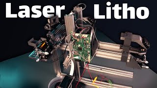
11:00 3D-printer photolithography
13:30 Physical Vapor Deposition (PVD)
15:52 Device operation
16:57 Black spot formation/degradation
18:50 Hermetic encapsulation
All technical details described in this video can currently be found in the public domain.
Video on the inventors of the OLED:
"Pioneers of OLED: The Ching Wan Tang and Steven Van Slyke Story"
• Pioneers of OLED: The ...
The original paper by Tang and van Slyke can be downloaded for $35 from:
aip.scitation.org/doi/pdf/10.....
I did not do this, so I hope my memory served me well...
Other sources used (fair use policy assumed):
Photo flexible OLED-display: pi-scale.eu
Photo plasma display: "History of the Plasma Display Panel" by Larry F Weber,
Photo Atari Lynx: boards.dingoonity.org/retro-gaming/atari-lynx-lcd-mod-by-mcwill/
Photo PVD: www.tekniker.es/en/pvd
Did I forget anyone / objections? Please let me know and I'll set it straight.
ITO substrates can be bought from many different suppliers on Ebay.com, with widely varying prices. I bought mine (5 pieces) from seller "yaolihong2013" (no affiliation) because the same shop also sells Ytterbium.
The AlQ3 and TPD were both bought from TCI-chemicals (no affiliation).
The 3D-printer used for the photoresist exposures was a Phrozen Sonic Mini 4K. Avoid the new update (1.9) of the Chitubox-software supplied with this printer because it does not work properly. Version 1.8 or earlier does works correctly.
Photoresist used : AZ 4533 supplied by Microchemicals (no affiliation)
Do you like what I do and want to support it? I'v recently started a patreon page: / huygens_optics  Наука
Наука


Some people got a bit angry, sad, or even emotional because of my rather cynical closing remark (which suggests planned obsolence of these devices). In a way, I guess that is a good thing, because I myself am very much against such practices. But unfortunately this remark also misses some of the nescessary nuance: with OLED devices it is still difficult to achieve the same long operational life times that we know from LCD -displays, due to the limited stability of some of the materials.
An aspect I should have added is that, even though it is possible to achieve very long shelf life in research by using exotic packaging methods, these methods can not always be transferred directly to mass production. For example, the metal seal shown in the video was made of a metal mixture that is unacceptable for production based on environmental considerations. Also, the packaging was quite expensive to manufacture.
When bringing a product to the market, the design is always the sum of considerations regarding quality, price and environmental impact. And since consumers nowadays are not always prepared to pay for quality, regrettably there is a lot of inferior products on the market.
An INCREDIBLE Video!!! I preferred people being upfront on what Could happen, then saying Good Luck, we build it to specs, and it fails later ( wait...why did I have a failed product ).
On a side note.... this probably explains why this happened to me on an OLED display in my home.
I think from your tone it should be obvious that you are not delighted by the practice of limited design life.
Thank you for making it a conversation point.
Planned obsolescence is when there is a better design choice for long life and it is NOT TAKEN, not when a marketing compromise has to be made.
I have 3 of the first commercial color portable oled devices, nokia n85(2008) galaxy s(2009) and Cowon s9 (2008). Nokia and galaxy used for 3 years maybe before storing in the shelf, cowon s9 almost continuous use for 12 years. None of them developed burn in, while a lot of my later oled phones did (galaxy s7 active likes to turn pinkish for example), i tried to find examples on the web of this devices getting burn in, very few in a decade.
I think the oled devices are long lived (so far), but samsung changed the chemical recipe at some point and the newer devices are more prone to burn in.
Show us how to perform lens coating! It is useful for camera refurbishment for lens coating damaged by fungus ...
I found none of those emotions when hearing that comment. It made me want to subscribe to hear more honest thoughts. I cant imagine how frustrating it must be to give somebody an innovation, and watch them dissemble it, remove the benefits, and use its mass appeal for profit.
Loving the content by the way. Thanks for showing me this procedure and making it easy to understand. And also thank you for explaining further on HOW one would make an item that truly lasts. It helped me understand why it is/was an exciting thing to be researching.
Really, really nice work putting this video together! The brightness of your oled is much higher than I'd expect. Now I'm curious about hole transport vs injection...
Thanks Ben. Concerning the difference between hole injection and transport layers: I'm not an expert on this, but I think the hole injection is specifically intended to match electrostatic potentials at the anode in order to create as many holes in the material as possible. The transport layer has a high P-type conductivity. So the voltage drop over the transport layer is relatively low and the field over the luminescent layer will be relatively high. In this way it is possible to inject a lot of holes into the electroluminescent layer and at the same time cause most of the recombination to take place in the luminescent layer.
ben! stop procrastinating on youtube and go to your lab!uploads something to as!!
I can see Ben now wanting to use his antique camera to make some high quality OLED masks. :)
Hey Ben, here is another valuable video ruclips.net/video/DL5jdmJi7k0/видео.html
@@capnthepeafarmer it occurred to me that the 35u pixels on the printer being too big might be a solvable problem with a macgyver setup of a fresnel lense and an objective...could get those pixels down to itty-bitty.
This is a throwback of a video. In college I took a lab where we made OLEDs in the same process described in the video. It was taught by my professor Dr. David Braun. He worked at Phillips in the early 90s in Europe. It is possible you worked with him.
Yes I do know David, I have worked with him at Philips. I think after his time at Philips he went back to Santa Barbara.
"Devices made for eternity aren't necessarily good for business" 😂
Love that line
_[Planned Obsolescence intensifies]_
This is an incredibly underrated statement in current society.. right to repair doesn't necessarily solve this problem in the realm of complex oled displays but it does help in reducing the waste from peripheral failures in the pcb's that power the oled displays and other electronics.
True capitalist story. :')
I subscribed during this video, unsubscribed after this phrase
@@jdpantoja442 the opposite idea would be stagnate with the same design forever, which is death. adapt or die. even biology, you can't escape that.
Even if I understand how OLED and lcd screens work I still can't believe how the hell we managed to push that technology to microscopic size and make hi-dense screens that push hundreds of pixels in space of one mm... The same with processors, we managed to squeeze so much transistors in such small space...
Also damn... I still sometimes think that 1990 was few years ago... We are old...
I watched this video in hopes of closing the perceived gap between OLED being science and not just magic. Seeing how much it took just to get a barebones low resolution single color display almost reinforces the belief that these OLED panels on phones and such are secretly magic. I'm not well studied in chemistry and electric engineering but I could understand the general concepts in this video, and I still have to take a huge leap of faith to believe my phone screen and TVs aren't just magic instead.
> _"how the hell we managed to push that technology to microscopic size"_
Lenses, lenses, lenses. Now, if only there was some RUclips channel about _those..._ ;-)
@@RFC-3514 Also lithography techniques from the semiconductor industry. The same idea is used to cram more transistors into CPUs.
@@CraigBrideau - _"A semiconductor lithography system undertakes a process whereby highly complex circuit patterns drawn on a photomask made of a large glass plate are _*_reduced using ultra-high-performance lenses_*_ and exposed onto a silicon substrate known as a wafer."_
@@RFC-3514 What they don't tell you is that they are actually pushing past the diffraction limit of those lenses using interferometric techniques! That's how you can get
When I was fifteen my mum was feed up with me always playing my records on the stereo in the living room. She promised me to pay half if I came up with the rest. This was November 86. I bought a Philips for £400. Record player, radio, double cassette and CD all integrated. It’s still working. I’ve changed the belts, but the motors are all fine. That’s quality for you.
When I grow up I wanna be a fireman!
You can still buy things that last, but you have to pay for them. Nobody wants to pay for them. People want cheap things they can just throw away, even if they say otherwise most of the time. Companies are merely giving us exactly what we are asking for. Simple.
" I’ve changed the belts" Philips nowdays is one of the big companies that are lobbing against 'right to repair'...
@@SuperAWaC You are only 99.99% wrong... its called planned obsolescence and it have nothing to do with your silly idea that you need to pay much more for products that are made with longevity in mind.
Most idiotic part of your idea is the fact that you think that it can be like that for ever because it is some kind of a law of mother nature or something.
We diging out our resources out of the Earth and then most of them are ending in massive pile of trash where they are considered irrecoverable... that can not last long as the resources of the Earth are limited!
No to mention that you "simply" advocating for some greedy share owners that are forcing us to pay multiple time for the same product... looks that you "simply" lack imagination to see that they are making a sucker out of you and suner or later everyone gonna need to pay for it when we will be forced to pay premium for the resources as they will be in huge pile of trash and it will be expensive to get them back out of it.
@@Bialy_1 The right to repair movement is misguided, and as it is now will only make things worse.
The fact that a channel of your caliber exists, amazes me every time.
What an absolute gift to have people like you on RUclips, explaining complex science to us plebs 😄
Oh wow, I worked as a contractor for Philips in Hamburg, Germany in the mid 90's before moving to the states. Video already got a like :-)
Wow! Your device looked great, and the explanations were really helpful! I understood how OLEDs worked at a very high level, but seeing all the intimate details really helped solidify how they _actually_ function, and filled in a lot of gaps (particularly the recombination of holes and electrons "inside" the organic layer, makes sense but never thought about that being the mechanism). Interesting to hear about the challenges of OLEDs and making them scalable. Seriously great work, thanks for sharing!
This man just happens to have his own thermal deposition setup. Absolutely amazing.
Problem of these days... "After all, devices made for eternity aren't necessarily good for business"
Yeah, a harrowing statement right at the end of the video. Capitalism showing it's utter wastefulness, planned obsolescence, and anti-environmental aspects. Still - amazing video, you're the new 'applied science' channel!
Yea, that made me feel rather sad despite how true it is.
I think it is more complicated than that. I have an old SonyEricsson smart phone. The LCD has developed a weird black blob on the bottom. It makes me sad. But, none of the cellular networks support 2G anymore, and it predates WiFi on phones. So I can’t do anything interesting on it.
If they’d done a better job making the display last longer, it wouldn’t have made the device last any longer in terms of usable life.
@@gf2e While those are good points, what you're describing is technological obsolescence (new tech is better and old tech is deprecated) instead of planned obsolescence (intentionally designed so that it has to be replaced by the same or very similar product).
Tech obsolescence despite being more nuanced (kinda bad but at least understandable), can still be mitigated if the intent for device longevity is there. At a minimum an old smartphone can still be used as an alarm clock for instance even if it no longer works as a phone. While some design intent into creating a longer lasting device may result in an upgradable or more feature full product.
I totally agree with the comments on my somewhat cynical remark at the end of the video. Personally, I really love older stuff that just keeps going, also from the environmental point of view.
Did my physics master's project on this technology over 20 years ago. You could count the amount of research papers on oleds with 2 hands. Instability and degradation was a big hurdle in the early devices, hope me and my fellow colleagues work was of some benefit.
Oh wow, I never thought to use my 3D printer to expose photoresist... this alone is going to streamline PCB prototyping and make very quick once off builds a complete joke for me to produce.
I can't thank you enough for that trick! It's so obvious now that I've seen it but I never put it together until you did it :O
Honestly, yeah it was such an obvious application
Obvious and yet here I was printing masks out like a fool, but no more!~
It's weird how the utterly obvious is so hard to reveal. Einstein is probably the best example of a mind that could look at reality and make the connections needed to reveal the fundamental obviousness extant in the universe. Like a fish not knowing that it lives its entire life suspended in a liquid.
Yeah, it's like SNAP. Now we need to find a way to rig 4k replacement screen from this printer to RPi. That should be such a wonderful device for PCB prototyping.
Genius idea _seems_ obvious but only after hearing about it
I'm struggling through a course in college on semiconductor theory and it's inspirational to see what you can actually do with the information if you understand it. Great presentation!
I absolutely *LOVE* this channel! Every episode is like a fresh injection of knowledge, inspiration and ambition to achieve.
I really admire a person like you that has the knowledge, the skill and the tools in his home to build a working OLED.
Great respect.
I love how much this feels like a lecture, in a good way
It's really impressive work. Huge thank you for documenting these processes.
This is a remarkable video, supremely informative without being overwhelming. Thanks for sharing your knowledge!
Sir, I do enjoy your videos very much! The best part of these, at least for me, is that even without a higher education or training in physics and/or electronics, I am still able to get the main idea of your very educating videos. Erg bedankt!!!
I just think it's amazing how much great educational material is made available by the technology and science RUclips community. It's work that really has a great impact on helping others learn more about the technology and phenomenon that play such large parts of our lives. Thank you for your work
Love the science overview here. Thank you for making this video. It is not easy to find informative videos on technologies from experts in the field.
I adore your channel! Never thought I’d see the day with real science happening on RUclips! In such a big way! Thank you.
My dad worked at a company for a while which worked on a brightness compensation algorithm for oled screens in the mid 2000s. As the oled ages it gets dimmer and they figured out a way to boost the voltage to compensate for this without causing bright/dark spots.
At some point this indeed might no longer compensate for the wear of the oled, I think modern OLEDs are generally a bit less susceptible to this?
Amazing to not just hear about but to actually see how an OLED works (and breaks down in air, if not properly sealed). Thanks very much for making this video!
An amazing video! I remember drooling over articles about OLED's in the 90's. Beautiful.
Making OLEDs at home... that's beyond awesome!
Great presentation. Even as someone with no professional nor higher academic experience in chemistry or physics (but a just a hobbyist interest these days) you very clearly explained the mechanism. Well done.
You have just the right amount of detail in the explanations, thank you for all your videos!
Wstching this on a foldable OLED screen and it just made appreciate it even more. Thank you for sharing your memories with us.
Finally got around to know how my phone's display is made. This is probably the most educational video I've seen so far
this channel is a goldmine. You are so good in explaining those concept very clearly.
I studied materials for thousands of hours at university as an engineering student but rarely excited on topics although all was scientific things. But seeing this video just reminded me how I love science in practice. Your video material is one of the best so far I ever watched. Thank you for sharing. Subscribed for more.
Your videos are amongst the most impressive I've ever seen on RUclips. Respect dude.
The method of using the 3d printer like that is probably the coolest thing I have seen all year.
love watching a pro do their thing, this is amazing! Big props
I have no idea, why this video was recommended to me but I absoluely love this information rich content here!
Your videos are so detailed and interesting yet easy to understand, I always learn something. Thank you.
Great video. Great channel all around. Such unique and enlightening content with no punches pulled on the technical details. Just the way I like it! Thanks for sharing your passion with us. Cheers.
When I'm recommended a video from a (relatively) small channel that's FULL of comments from my absolute favorite channels I know I've found something special. :)
Fascinating video! Always great to see technology like this being within reach of average people (outside of a large lab). Thank you so much for this!
Thank you for showing us your work and taking the time to explain it.
What an amazing video on an equally amazing topic! So glad that I found your channel half a year ago.
This stuff is so cool! I am very glad that I stumbled upon your channel a while back and I'm also really grateful for your channel and a the uploads!
Love your explanation of the OLED manufacturing engineering. Learned something today! Thank you.
This is the best tutorial I seen on making OLED think your very much for taking the time to do this.
I have only just found your channel - The explanations and demonstrations are absolutely fantastic. Thank you.
What an excellent video!! The theoretical and the experimental sides of it are just perfect complement to each other!
Wow, I'm really glad I found this channel. This is some great stuff. I'm looking forward to more. Cheers.
Thank you for bringing us the tech that everyone take it for granted.
Very impressive! I never thought that I would learn so much about OLED technology in such a short timespan.
Cool video. I did an internship at TNO in Eindhoven working on similar things in 2006. I remember the samples always degrading quickly. That's so nice you can make these in your home setup
Nice to watch a video that is not dumbed down at all (or if it is, it is to my level ;-). Also, the pace is nice as there is enough content there as well - so many videos on RUclips I watch at 1.5 or 1.75 times the speed because they are so slow. It is a pity that I have other things to do and have to limit myself to watching only one of these a day (now that I have discovered that your channel exists) otherwise, I would certainly binge-watch them and lose a lot of time. Keep up with these excellent videos.
Great video, I enjoyed it a lot. I need to present to my class on the working principle of OLEDs and this was very helpful in building my understanding.
Very impressive technology. Watching this on the OLED screen of my phone, where pixels are so tiny that I cannot see them by eye.
The video helped me understand the mechanism of hole and electrons meeting each other in the Laye and emitting light. thank you very much
Great project and excellent video! Very informative and a pleasure to watch!
Holy smokes, what a great video!
So information dense, yet I was able to understand it all. You taught me a lot in a short time. Thank you.
Wow! Thank you for preserving this institutional knowledge and taking the time, effort and expense to give example.
I never thought id learn this much about OLEDs. Very good video!!
This is what a real inventor looks like. Thank you
This is hands-down the best high-tech science channel on YT.
This is amazing. I remember reading about OLED in Scientific American back in 2004. It talked about making flexible display out of it. Almost 20 years later, we now have phones that have flexible displays.
This channel is really amazing! Thanks for sharing all your inventions!!
nice production , great lesson. Thank you so much for making such a great experiment on OLED displays !
You just won my subscription! Great work. Very good explanations.
When i saw the thumbnail, i got the catch, when i saw the "wood-walk" even for a second, i know i am in a good place! Thanks for the thecnological progress!!!
fantastic demo work, thanks, and to see the oxidation is great
I really liked the zoomed microscope shots that showed the degradation of the device. Surreal!
Excellent, Ive always wondered how an OLED was constructed, thank you for sharing this
Really clever using the resin printer to make the photoresist pattern. Great video!
Very informative video. The main thing is the processing steps and you well defined them in your own facility. Appreciable. 👍👍
Oh WOW! How I wish YOU had been my chemistry/physics teacher at college.
I feel like I learned more in the last 20mins than I did in a whole year at college. Thank you.
Going to look at your other videos now and will most likely subscribe.
Regards Mark in the UK
Great to go down this memory lane with you good sir. o7
Amaizing, thats why you are such a wonderful experimentalist ( former phillips researcher!)
You are a kind of hero for me, I have readed a lots of articles on the subject dreaming some day do it myself.
Thanx for sharing, greetings from a small town in México.👍👍👍
Hola, Francisco...... It was an Incredible video, I hope that you can replicate this work, for me I don't have the ability nor the equipment to do such a-thing. But All the best to you in your work / Buena Suerte en su trabajo!!
From a Big city in California!!
Wow! That was some serious video! Thank you so much for getting into the trouble of describing the barriers. Subscribed.
Fascinating watch, thank you for working on this.
I watched this video with genuine respect to you. Such an ease of explaining complex science that lies behind the OLED's working principle! I actually do research on OLEDs and organic photovolatics - I think I kinda resemble you from the 90s, haha! Greetings from Łódź, Poland :))
Wow that was incredibly cool. I learned stuff about OLED displays I wasn't even aware I didn't know yet.
Very interesting and instructive video, especially regarding the shortcomings of this technology
This is gold, extremely interesting, thank you for sharing your experience sir!
Thanks for the video! It's so interesting to hear from someone who actually worked with it. :)
Великолепный опыт, замечательное видео! Спасибо что позволяете нам так наглядно прикоснуться к таким сложным и интересным вещам! (Great experience, great video! Thank you for letting us so clearly touch such complex and interesting things! )
Great history review, explanation and very cool OLED project! 👍
Extremely interesting video, and I would say you definitely still have what it takes to make a great OLED!
Well structured and explained video, Thanks !
Such a great explanation. Much thanks for this video!
Wow, super nice results and using a resin printer to expose it was so clever!
Also for me a trip down memory lane as I have worked at Aixtron before, developing deposition machines for OLED production. Was a great time!
That was a very impressive lecture. Thank you!
Many thanks for your great videos. From South Africa. 👍👊
Thank you for your contributions.
I have always been fascinated with LED’s and it’s technology since I was in high school in 82.
It’s only the past year I’ve gotten back to basics with electronics again. How things have changed.
Very impressive fab steps and problem-solving in the process!
i think your kids must be incredibly grateful to have a father like you
Very interesting and informative video! I've learned a lot, and it felt more like 5 minutes than 20.
You are one of the coolest dudes I've ever had the pleasure to hear explain a subject.
Please tell that to my kids ;-)
Enthusiasm and well voiced. I always wanted to learn what makes a clean room what it is and to work in lithography for futuristic displays and interferometry. Your work from seven months ago on Logic circuits of light also very neat.. .
Awesome video. This is the kind of tech video I love to see.
Great video and explanation of the process!