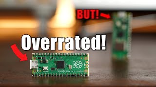
PI PICO W SILICON LEVEL TEARDOWN
HTML-код
- Опубликовано: 11 сен 2024
- The Raspberry Pi Pico gets a wireless interface! A good assembly to tear down as it shows the typical types of integrated circuits found on a modern circuit board and some state-of-the-art packaging technologies.
More details here: electronupdate...
Raspberry Pi Pico W


This channel is one of youtube's hidden gems.
Glad to see another video from you. Thanks for making these!
good to see you back
I always enjoy your Silicon Teardowns.
Would love to see more :)
That's super impressive to see. And you're incredibly knowledgeable about all the individual sections! Excellent work!
Welcome back!
Awesome
These are always so fascinating. I've often wondered what pathway does one take to get into the silicon level of engineering? It honestly seems like black art with VERY little information about it. From colleges, to classes, etc. The entire pathway seems almost secretive.
I would guess it is via FPGA like stuff and then to custom material from a foundry.
But that doesn't bring you custom transistors, but that kind of work is also done at universities.
I think electrical engineering, possibly masters level: I had undergrads working in my lab during grad school who had "intro to VLSI design" (which is basically what your question is, at least to start) textbooks.
For analog or layout design, try to get some qualification from university for electronic engineering and then get hired as a junior. You will learn most of everything on the job.
Digital design is a bit different. With FPGAs you can teach yourself how it works to some level. Timing and simulation will be a lot different for digital directly placed on silicon though.
We missed you
Glad to see you back. What kind of acid do you use and what percent concentration
Do you know if the programmable I/O (PIO) function of the pico is somehow structurally visible (clearly) or just part of the very dense "verilog" block? I suspect the latter. There should be 8 PIO statemachines/processors.
Fantastic die shots with the metalization removed! Always impresses me not only how complex WiFi is but that all of that functionality can be almost entirely on die and manufactured for so little.
I do wonder how the Pico ASIC die was packaged during development, I doubt it was a bog standard plastic QFN, maybe some manually wire-bonded gold/ceramic hybrid DIP or PGA carrier?
I work at a semiconductor company that develops ASICs containing ARM microcontroller cores and custom mixed-signal IP. They're all packaged in the "production" packages (usually QFN) during development. Digital stuff usually gets prototyped on FPGAs first.
If we need to test changes to the actual silicon design during development, we send the packaged chips out to another company that decaps them and uses focused ion beam (FIB) micro machining to edit the chip.
@@twicecookedpork6220 Thanks for the info! I guess if you're going to the effort of making masks and entire wafers they're probably quite far into development so you might as well test them in their intended package?
@@WizardTim Yes. The cost of mask sets at 40nm or 22nm as used on many micros is quite high. Much better to go the FPGA route (and backed up by simulation) and then go to the real thing at the correct physical size. Packaging can have a big impact on device characteristics.
Yas, love these videos. So interesting.
We'd love to see you at least once desoldering and decapping the chips!
Antenna design is a mix of voodoo and black magic. At a previous employer, we made some 50 different PCB antenna designs, to test and see what would work out and I think two of them were acceptable, but none of them good...
The Pi 4 has the text "Uses technology licensed from Proant AB" on the PCD near the antenna...
@@pizzablender yeah, it's a Swedish company that seems to specialise in antenna designs.
Speaking of Raspberry Pis, could you give us an update on your buried file server?
Initially I thought they added wifi by simply slapping a second microcontroller under the can next to the rp2040. Thanks for the great teardown, does seem like a peripheral device (although comments below suggest it still has a bunch of ARM cores).
I hope in the future more videos will be uploaded
This is the same AIROC wireless ASIC used in Laird's inexpensive Sterling LWB+ industrial WiFi modules.
I'd love to know how you expose the die so cleanly. I copied a method which involves using glass etching paste to dissolve the copper layer which works well but never looks perfect (like yours)
Hey, I Just sent you an email today. I don't know if you don't check that email address anymore because it got filled with spam?
It was like techno-porn..