@@DjaniAgain A lot of them are redundant pins to help mitigate things like interfacial voiding and thermal stress to increase the lifespan of the component.
Too bad these are all flip chips… the cool metallization layers on the silicon die are all facing down so they are burned off last. Would be cool to remove the die from the board first and then do this!
This one is Intel T2300E, you are not far away. I checked and there are models shipped with T1700, which I believe is about the, just with lower specs.
In future I could make a tour, for now I will write about my setup and some settings! This is a desktop type fiber laser, it is a generic Chinese one, so it has no brand, no medel written otside 😒, believe me, 50W output power! Thats it! 😅 The software is EZCAD Line distance is set to 0.031 mm Speed is around 1300 mm/s Power: between 20% and 80% Frequency: 30 kHz
I'm not too sure if it will work. In the video with the Optocouplers, you can see the laser-treated surfaces closely. They become abrasive, i.e. this will reduce the contact area of the CPU with the heatsink. Here is the part from this video: ruclips.net/video/9xp7JhVqIBE/видео.html
Hard to remove 1 layer of copper. It depends, what is the purpose, and you can adjust power to do gentle peeling or burn as much as possible. On this processor first few passes were at about 30% of 50W fiber laser.


Chat GPT is scared of this
🤣😂😅
😁😁😁🤣🤣🤣
😅
Maybe Chat GPT will behavior like cyberdine (Terminator) in the future hehe
✌️
I love how most of the chip's area is just wires to the actual processor
With 90W TDP, no wonder there's two big traces going into and out
It's amazing how many pins there are under the die 🤯
ruclips.net/video/BSbQV6Be79s/видео.html
I guess half of them are for powering the chip 🤔
@@DjaniAgain A lot of them are redundant pins to help mitigate things like interfacial voiding and thermal stress to increase the lifespan of the component.
👌 Thank you for info my friend ✌️
Linus tech should try to solder wires on such ic
Play this video in reverse and you'll have alien repair ray 😃.
😱 Interesting observation ✌️
Thank you my friend!
"Do you expect me to talk?"
"No Mr. Bond, I expect you to die!"
😅😂🤣
This laser humiliates everything, but in the middle of the processor there is a thick copper layer for cooling?
I really don't know what it is, but it is tough 😅
That is the die of the cpu it self not copper
It's the actual silicon
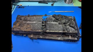
What is inside a Laptop processor ?
Here is part 2: ruclips.net/video/RrjltzBoS1o/видео.html
And part 3: ruclips.net/video/BSbQV6Be79s/видео.html
cpu be like "thx master..i can now do 5 ghz on 1 pin"
😅😂🤣
Too bad these are all flip chips… the cool metallization layers on the silicon die are all facing down so they are burned off last. Would be cool to remove the die from the board first and then do this!
Awesome, thanks.👍👍👍👍👍
Thank you too!
That is an Intel Core Duo laptop CPU. I know because I have 5,084 of them as well as other Intel mobile CPUs on the wall in my office.
5000 processors on the wall 😳
Must be a very cool sight 🤔
Here is a good idea to make nice key-holder ;)
Yes, good idea actually
Looks a lot like the CPU i pulled out of a lenovo ThinkPad R500 😅
This one is Intel T2300E, you are not far away. I checked and there are models shipped with T1700, which I believe is about the, just with lower specs.
Would love to see this with an eye ball of refugee.
✌️
could this be used to reprocess the chip and recover the precious metals?
I think this would help!
Would be a terribly expensive way to go about it. Removing the epoxy and heating the chip die up in an oven would be just as good.
What setup do you use? What power is the laser? Can you give a tour?
In future I could make a tour, for now I will write about my setup and some settings!
This is a desktop type fiber laser, it is a generic Chinese one, so it has no brand, no medel written otside 😒, believe me, 50W output power! Thats it! 😅
The software is EZCAD
Line distance is set to 0.031 mm
Speed is around 1300 mm/s
Power: between 20% and 80%
Frequency: 30 kHz
Is there gold remaining?
I'm not sure 🤔
core 2 duo t2300e CPU @ 1.66GHz
Yes, you are totally right ✌️
@@DjaniAgain thanks
intel me debloating be like
✌️
Было бы не лишним смахивать пыль после каждого прохода лазера 😉👍🏻
Interesting idea 🤔
Можно так скальпирование проводить, для большего охлаждения и более тонкого контакта с охлаждением 😄
I'm not too sure if it will work.
In the video with the Optocouplers, you can see the laser-treated surfaces closely.
They become abrasive, i.e. this will reduce the contact area of the CPU with the heatsink.
Here is the part from this video: ruclips.net/video/9xp7JhVqIBE/видео.html
В конце выглядит довольно рабочим 😀
✌️
What wattage laser is that?
50 watt my friend!
Zoom 2000x white microsope please
How many pcb layers is it removing with every pass?
Also 4:37 are those small lines standing up cpu traces/wires?
Yep!
Hard to remove 1 layer of copper. It depends, what is the purpose, and you can adjust power to do gentle peeling or burn as much as possible. On this processor first few passes were at about 30% of 50W fiber laser.
Que bonito llavero, si lo usaría asi
Awesome idea! ✌️
Multi layer pcb
You should remove the flip chip and burn off the ball layer
I tried this too, wait for results on future videos
I aggree...this video is not full
Residente evil 😮😍
✌️
Try a Mobile phone Processor..love see it..
There is one!
6:28
ruclips.net/video/uMi_9sXX8mU/видео.html
Под I9 перемаркировать и продать)))
😁🤣😜
Нихрена у меня 3090ti и чип GP 102 он очень большой !!!
✌️
Pleas zoom with microscope
My latest video is a follow-up, please watch it. There is more zoom, but not on the board itself! ✌️
its a big failure LOL you have destroy Copper plate conection . the chips is alive LOL fails !