Most Important PCB terminologies

HTML-код
- Опубликовано: 7 июн 2021
- Altium Designer trial link - www.altium.com/yt/gadgetronicx
Most important PCB terminologies to be aware of. In this video we will explain PCB terminologies and why it is so important to understand them. Some of the important terminologies are
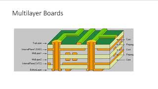
1. Layers
2. Copper tracks
3. Trace width
4. Vias
5. Copper areas
6. Footprint
7. Silk screen
8. Board dimensions
For more Guides, Projects, Circuits and tutorials visit - www.gadgetronicx.com


Perfect! Clear, structured, informative, and best of all: no music! Music interfers with the speaker's voice.
Glad it helped!
That type of explanation is required ❤ it is very impressive and simple to understand
❤️
Very nice
Thank you :)
Nice video 👌 please upload videos on layer stack in pcb Design
Thank you, will do