
- Видео 2
- Просмотров 99 822
Solahuddin Jr
Добавлен 1 апр 2012
Video CV
Muhammad Solahuddin Sayudzi
UiTM Shah Alam, Selangor (MY)
*pardon me,there were some mistakes on pronunciation*
UiTM Shah Alam, Selangor (MY)
*pardon me,there were some mistakes on pronunciation*
Просмотров: 228
Видео
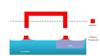

CMOS Fabrication Process (Animation)
Просмотров 100 тыс.7 лет назад
Gonzalez Margaret Harris Betty Brown Maria
very nice explanation
one of the best explanations
1000 likes 🎉🎉
mind fcuk
thnaks dude
I want this animation please send me
A brilliant Video. Very well done. Very talented. It's interesting that oxide is needed for N+ diffusion but not for P+ diffusion. Why is that? I think oxide is needed in both cases. Also photoresist is used in every stage of masking. You have shown it only for Nwell deposition
can i know what editor did you used to make this animation?
Hi. I used Sony Vegas to create this animation. Since no sound added in, so it was just a simple one.
Really intuitive and visual way to explain it, great work and thank you.
Due to COVID19 Pandemic colleges are not opening and I can't access the cadence software so I searched for an open source software and I found GLADE. Check out my playlist on Layout Designing using GLADE. #LearnFromHome VLSI Layout Designing using GLADE (Open Source Software) Playlist Link:- ruclips.net/p/PLWcG9vtrFH0YVZvd3yf2Xmm_Gl0y-XXz6 Video 1: All the CMOS Design Rules are explained. Video 1 link: ruclips.net/video/b3IlK1WZIHA/видео.html Video 2&3: Glade Downloading, Setup and Configuration. Video 2 link: ruclips.net/video/LMZ3O6Akfro/видео.html Video 3 link: ruclips.net/video/1ueSinMmqkA/видео.html Video 4: Designing Layout of nMOS and pMOS is explained. Video 4 link: ruclips.net/video/oOblwp65WFA/видео.html Video 5: Designing CMOS Inverter Layout using 1 metal layer is explained in detail. Video 5 link: ruclips.net/video/Qr0nTPo-Ri0/видео.html Video 6: Verification of Designed Inverter Layout using LT Spice. Video 6 link: ruclips.net/video/kvrF6Zv6Y_U/видео.html Video 7: Designing CMOS Inverter Layout by using 2 metal layers and Vias. Video 7 link: ruclips.net/video/HZopqROB2GA/видео.html Video 8: Designing 2 Input CMOS NAND Gate. Video 8 link: ruclips.net/video/41067AYX_do/видео.html Video 9: Verification of Designed NAND Gate Layout using LT Spice. Video 9 link: ruclips.net/video/3pufZ6InuHQ/видео.html Video 10: Designing 2 Input CMOS NOR Gate. Video 10 link: ruclips.net/video/skYC2UnJgQ4/видео.html Kindly Like, Share among your engineering friends so that they can also learn from home and subscribe to my Channel for more GLADE Tutorials. Your Support will be appreciated. Thank You
It's really awesome explanations 👍
Informative
too goood
nice one, but in the last forgot to make contacts of gates, i.e., polysilicon also covered with SiO2
how can you do P-diffusion on specific area without defined the active area by using some kind of mask?
You are right. It was an oversight on his part. Also photoresist is used in every case of masking
a quick and easy way to understand the process...really appreciate it
Best... Among all videos
Well prepared
A Japanese engineer, a long time ago, told us that CMOS is like making layered cake! But first you must know what kind of IC chip design you want and then proceed to create a plan on how to make it from bottom to top by a simple layering technique. Today with the use of combined maskless ion beam lithography and maskless electron beam lithography using guiding guidance lasers to help pin point precisely where and when to start and end the deposition and welding process combined with precision servo-mechanisms the CMOS cake layering bottom-to-top technique has become quite easy but you must start first by using larger size components and simple designs and compensate by using a much larger silicon chip which is almost the size of a large ID card.
That’s the longest run on sentence I’ve ever read. Lol
@@jeffdaidiot Somebody has to say it and write dow in that way for non-scientists and non-engineers and for non-technologists and for non-technically oriented but VERY CURIOUS PEOPLE who wants to know more but are just too afraid to ask the questions that they have without being ridiculed by the specialists and experts. A good teacher must know how to make something really understandable to EVERYONE regardless of their educational background. In that way, you can and will attract people into this field of engineering and technology. By the way, I was once a temporary teacher in the 1990s after my retirement in the 1990s.
@@darthvader5300 bruh!!
Very simple easy to understand your video is osm for last minute recall.
Good explained...🙌🙋..Upload more videos
Can you share document in text form ! thank you huongvbhp93@gmail.com